ZHCSGF6A April 2017 – July 2017 TPD2S701-Q1
PRODUCTION DATA.
- 1 特性
- 2 应用
- 3 说明
- 4 修订历史
- 5 Pin Configuration and Functions
-
6 Specifications
- 6.1 Absolute Maximum Ratings
- 6.2 ESD Ratings—AEC Specification
- 6.3 ESD Ratings—IEC Specification
- 6.4 ESD Ratings—ISO Specification
- 6.5 Recommended Operating Conditions
- 6.6 Thermal Information
- 6.7 Electrical Characteristics
- 6.8 Power Supply and Supply Current Consumption Chracteristics
- 6.9 Timing Requirements
- 6.10 Typical Characteristics
- 7 Parameter Measurement Information
- 8 Detailed Description
- 9 Application and Implementation
- 10Power Supply Recommendations
- 11Layout
- 12器件和文档支持
- 13机械、封装和可订购信息
封装选项
机械数据 (封装 | 引脚)
散热焊盘机械数据 (封装 | 引脚)
- DSK|10
订购信息
11 Layout
11.1 Layout Guidelines
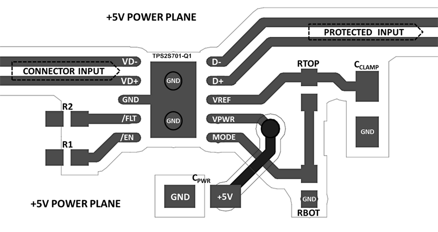
Proper routing and placement maintains signal integrity for high-speed signals. The following guidelines apply to the TPD2S701-Q1:
- Place the bypass capacitors as close as possible to the VPWR and VREF pins. Capacitors must be attached to a solid ground. This minimizes voltage disturbances during transient events such as ESD or overcurrent conditions.
- High speed traces (data switch path) must be routed as straight as possible and any sharp bends must be minimized.
Standard ESD recommendations apply to the VD+, VD- pins as well:
- The optimum placement is as close to the connector as possible.
- EMI during an ESD event can couple from the trace being struck to other nearby unprotected traces, resulting in early system failures.
- The PCB designer must minimize the possibility of EMI coupling by keeping any unprotected traces away from the protected traces which are between the TVS and the connector.
- Route the protected traces as straight as possible.
- Eliminate any sharp corners on the protected traces between the TVS and the connector by using rounded corners with the largest radii possible.
- Electric fields tend to build up on corners, increasing EMI coupling.
11.2 Layout Example
 Figure 24. TPD2S701-Q1 Layout