ZHCSGF6A April 2017 – July 2017 TPD2S701-Q1
PRODUCTION DATA.
- 1 特性
- 2 应用
- 3 说明
- 4 修订历史
- 5 Pin Configuration and Functions
-
6 Specifications
- 6.1 Absolute Maximum Ratings
- 6.2 ESD Ratings—AEC Specification
- 6.3 ESD Ratings—IEC Specification
- 6.4 ESD Ratings—ISO Specification
- 6.5 Recommended Operating Conditions
- 6.6 Thermal Information
- 6.7 Electrical Characteristics
- 6.8 Power Supply and Supply Current Consumption Chracteristics
- 6.9 Timing Requirements
- 6.10 Typical Characteristics
- 7 Parameter Measurement Information
- 8 Detailed Description
- 9 Application and Implementation
- 10Power Supply Recommendations
- 11Layout
- 12器件和文档支持
- 13机械、封装和可订购信息
封装选项
机械数据 (封装 | 引脚)
散热焊盘机械数据 (封装 | 引脚)
- DSK|10
订购信息
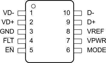
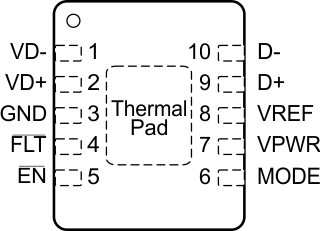
5 Pin Configuration and Functions
DGS Package
10-Pin SSOP
Top View

DSK Package
10-Pin QFN
Top View

Pin Functions
| PIN | TYPE | DESCRIPTION | |
|---|---|---|---|
| NO. | NAME | ||
| 1 | VD– | I/O | High voltage D– USB data line, connect to USB connector D+, D– IEC61000-4-2 ESD protection |
| 2 | VD+ | I/O | High voltage D+ USB data line, connect to USB connector D+, D– IEC61000-4-2 ESD protection |
| 3 | GND | Ground | Ground pin for internal circuits and IEC ESD clamps |
| 4 | FLT | O | Open-drain fault pin. See Table 1 |
| 5 | EN | I | Enable active-low input. Drive EN low to enable the switches. Drive EN high to disable the switches. See Table 1 for mode selection |
| 6 | MODE | I | Selects between device modes. See the Detailed Description section. Acts as LDO reference voltage for mode 1 |
| 7 | VPWR | I | 5-V DC supply input for internal circuits. Connect to internal power rail on PCB |
| 8 | VREF | I/O | Pin to set OVP threshold. See the Detailed Description section for instructions on how to set OVP threshold |
| 9 | D+ | I/O | I/O protected low voltage D+ USB data line, connects to transceiver |
| 10 | D– | I/O | Protected low voltage D– USB data line, connects to transceiver |