SLVS615F July 2006 – December 2016 TPD4E002
PRODUCTION DATA.
8 Application and Implementation
NOTE
Information in the following applications sections is not part of the TI component specification, and TI does not warrant its accuracy or completeness. TI’s customers are responsible for determining suitability of components for their purposes. Customers should validate and test their design implementation to confirm system functionality.
8.1 Application Information
The TPD4E002 device is a TVS diode array typically used to provide a path to ground for dissipating ESD events on high-speed signal lines between a human interface connector and a system. As the current from ESD passes through the TVS, only a small voltage drop is present across the diode. This is the voltage presented to the protected integrated circuit (IC). The triggered TVS holds this voltage, VCLAMP, to a safe level for the protected IC.
8.2 Typical Application
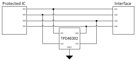
In a typical design example, one TPD4E002 device is being used to protect an IC against potential ESD from a four-channel human interface port, as shown in Figure 4.
 Figure 4. Typical Application for TPD4E002
8.2.1 Design Requirements
Table 1 lists the parameters for this typical application.
Table 1. Design Parameters
| DESIGN PARAMETER | VALUE |
|---|---|
| Signal's voltage range on I/O1, I/O2, I/O3, and I/O4 | 0 V to 5 V |
| Operating frequency | < 100 MHz |
8.2.2 Detailed Design Procedure
To begin the design process, some parameters must be decided upon; the designer must know the following:
- Voltage range of the signal on all protected lines
- Operating frequency on all protected lines
8.2.2.1 Signal Range on I/O1 Through I/O2
The TPD4E002 device has 4 identical protection channels for signal lines. The symmetry of the device provides flexibility when selecting which of the four I/O channels will protect which signal lines. Any I/O supports a signal range of 0 V to 5 V and up to 100 MHz.
8.2.3 Application Curves
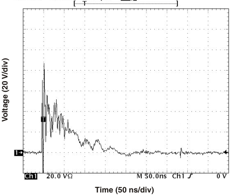
 Figure 5. ESD Clamp Voltage at I/O Pins: IEC6100-4-2
15-kV Contact Discharge
