ZHCSDD8D October 2014 – December 2019 TPS1H100-Q1
PRODUCTION DATA.
- 1 特性
- 2 应用
- 3 说明
- 4 修订历史记录
- 5 Pin Configuration and Functions
- 6 Specifications
-
7 Detailed Description
- 7.1 Overview
- 7.2 Functional Block Diagram
- 7.3
Feature Description
- 7.3.1 Accurate Current Sense
- 7.3.2 Programmable Current Limit
- 7.3.3 Inductive-Load Switching-Off Clamp
- 7.3.4
Full Protections and Diagnostics
- 7.3.4.1 Short-to-GND and Overload Detection
- 7.3.4.2 Open-Load Detection
- 7.3.4.3 Short-to-Battery Detection
- 7.3.4.4 Reverse-Polarity Detection
- 7.3.4.5 Thermal Protection Behavior
- 7.3.4.6 UVLO Protection
- 7.3.4.7 Loss of GND Protection
- 7.3.4.8 Loss of Power Supply Protection
- 7.3.4.9 Reverse Current Protection
- 7.3.4.10 Protection for MCU I/Os
- 7.3.5 Diagnostic Enable Function
- 7.4 Device Functional Modes
- 8 Application and Implementation
- 9 Power Supply Recommendations
- 10Layout
- 11器件和文档支持
- 12机械、封装和可订购信息
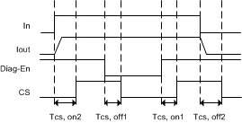
6.6 Timing Requirements – Current Sense Characteristics(1)
| MIN | NOM | MAX | UNIT | |||
|---|---|---|---|---|---|---|
| tCS,off1 | CS settling time from DIAG disabled | VIN = 5 V, Iload ≥ 5 mA. VDIAG_EN from 5 to 0 V. CS to 10% of sense value. | 10 | µs | ||
| tCS,on1 | CS settling time from DIAG enabled | VIN = 5 V, Iload ≥ 5 mA. VDIAG_EN from 0 to 5 V. CS to 90% of sense value. | 10 | µs | ||
| tCS,off2 | CS settling time from IN falling edge | VDIAG_EN = 5 V, Iload ≥ 5 mA. IN from 5 to 0 V. CS to 10% of sense value. | 10 | µs | ||
| VDIAG_EN = 5 V, Iload ≥ 5 mA. IN from 5 to 0 V. Current limit triggered. | 180 | µs | ||||
| tCS,on2 | CS settling time from IN rising edge | VVS = 13.5 V, VDIAG_EN = 5 V, Iload ≥ 100 mA. VIN from 0 to 5 V. CS to 90% of sense value. | 150 | µs | ||
(1) Value specified by design, not subject to production test.
 Figure 2. CS Delay Characteristics
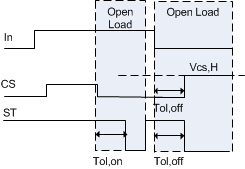
  Figure 3. Open-Load Blanking Time Characteristics
  Figure 4. Pin Current and Voltage Conventions