ZHCSDD8D October 2014 – December 2019 TPS1H100-Q1
PRODUCTION DATA.
- 1 特性
- 2 应用
- 3 说明
- 4 修订历史记录
- 5 Pin Configuration and Functions
- 6 Specifications
-
7 Detailed Description
- 7.1 Overview
- 7.2 Functional Block Diagram
- 7.3
Feature Description
- 7.3.1 Accurate Current Sense
- 7.3.2 Programmable Current Limit
- 7.3.3 Inductive-Load Switching-Off Clamp
- 7.3.4
Full Protections and Diagnostics
- 7.3.4.1 Short-to-GND and Overload Detection
- 7.3.4.2 Open-Load Detection
- 7.3.4.3 Short-to-Battery Detection
- 7.3.4.4 Reverse-Polarity Detection
- 7.3.4.5 Thermal Protection Behavior
- 7.3.4.6 UVLO Protection
- 7.3.4.7 Loss of GND Protection
- 7.3.4.8 Loss of Power Supply Protection
- 7.3.4.9 Reverse Current Protection
- 7.3.4.10 Protection for MCU I/Os
- 7.3.5 Diagnostic Enable Function
- 7.4 Device Functional Modes
- 8 Application and Implementation
- 9 Power Supply Recommendations
- 10Layout
- 11器件和文档支持
- 12机械、封装和可订购信息
6.7 Switching Characteristics
VVS = 13.5 V, Rload = 10 Ω, over operating free-air temperature range (unless otherwise noted)(1)| PARAMETER | TEST CONDITIONS | MIN | TYP | MAX | UNIT | |
|---|---|---|---|---|---|---|
| td,ON | Turn-on delay time | IN rising edge to VOUT = 10%, DIAG_EN high | 20 | 50 | µs | |
| td,OFF | Turn-off delay time | IN falling edge to VOUT = 90%, DIAG_EN high | 20 | 50 | µs | |
| dV/dtON | Slew rate on | VOUT = 10% to 90%, DIAG_EN high | 0.1 | 0.5 | V/µs | |
| dV/dtOFF | Slew rate off | VOUT = 90% to 10%, DIAG_EN high | 0.1 | 0.5 | V/µs | |
| Slew rate on and off matching | –0.15 | 0.15 | V/µs | |||
(1) Value specified by design, not subject to production test.
 Figure 5. Switching Characteristics Diagram
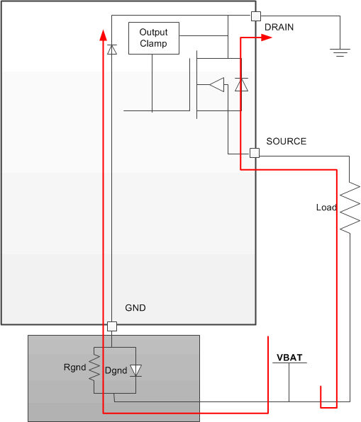
  Figure 7. Irev2 Test Condition