ZHCSDD8D October 2014 – December 2019 TPS1H100-Q1
PRODUCTION DATA.
- 1 特性
- 2 应用
- 3 说明
- 4 修订历史记录
- 5 Pin Configuration and Functions
- 6 Specifications
-
7 Detailed Description
- 7.1 Overview
- 7.2 Functional Block Diagram
- 7.3
Feature Description
- 7.3.1 Accurate Current Sense
- 7.3.2 Programmable Current Limit
- 7.3.3 Inductive-Load Switching-Off Clamp
- 7.3.4
Full Protections and Diagnostics
- 7.3.4.1 Short-to-GND and Overload Detection
- 7.3.4.2 Open-Load Detection
- 7.3.4.3 Short-to-Battery Detection
- 7.3.4.4 Reverse-Polarity Detection
- 7.3.4.5 Thermal Protection Behavior
- 7.3.4.6 UVLO Protection
- 7.3.4.7 Loss of GND Protection
- 7.3.4.8 Loss of Power Supply Protection
- 7.3.4.9 Reverse Current Protection
- 7.3.4.10 Protection for MCU I/Os
- 7.3.5 Diagnostic Enable Function
- 7.4 Device Functional Modes
- 8 Application and Implementation
- 9 Power Supply Recommendations
- 10Layout
- 11器件和文档支持
- 12机械、封装和可订购信息
7.3.4.2 Open-Load Detection
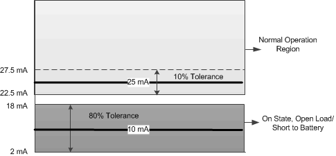
In the on state for version A, if the current flowing through the output is less than Iol,on, the device recognizes an open-load fault. For version B, faults are diagnosed by reading the voltage on the CS pin and judged by the user. A benefit of high-accuracy current sense down to a verylow current range, this device can achieve a very low open-load detection threshold, which correspondingly expands the normal operation region. TI suggests 10 mA as the upper limit for the open-load detection threshold and 25 mA as the lower limit for the normal operation current. In Figure 35, the recommended open-load detection region is shown as the dark-shaded region and the light-shaded region is for normal operation. As a guideline, do not overlap these two regions.
 Figure 35. On-State Open-Load Detection and Normal-Operation Diagram
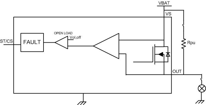
 In the off state, if a load is connected, the output voltage is pulled to 0 V. In the case of an open load, the output voltage is close to the supply voltage, VS – VOUT < Vol,off. For version A, the ST pin goes low to indicate the fault to the MCU. For version B, the CS pin is pulled up to VCS,h. There is always a leakage current Iol,off present on the output, due to the internal logic control path or external humidity, corrosion, and so forth. Thus, TI recommends an external pullup resistor to offset the leakage current. This pullup current should be less than the output load current to avoid false detection in the normal operation mode. To reduce the standby current, TI recommends always to use a switch in series with? the pullup resistor. TI recommends Rpu ≤ 15 kΩ.
 Figure 36. Open-Load Detection Circuit