ZHCSDD8D October 2014 – December 2019 TPS1H100-Q1
PRODUCTION DATA.
- 1 特性
- 2 应用
- 3 说明
- 4 修订历史记录
- 5 Pin Configuration and Functions
- 6 Specifications
-
7 Detailed Description
- 7.1 Overview
- 7.2 Functional Block Diagram
- 7.3
Feature Description
- 7.3.1 Accurate Current Sense
- 7.3.2 Programmable Current Limit
- 7.3.3 Inductive-Load Switching-Off Clamp
- 7.3.4
Full Protections and Diagnostics
- 7.3.4.1 Short-to-GND and Overload Detection
- 7.3.4.2 Open-Load Detection
- 7.3.4.3 Short-to-Battery Detection
- 7.3.4.4 Reverse-Polarity Detection
- 7.3.4.5 Thermal Protection Behavior
- 7.3.4.6 UVLO Protection
- 7.3.4.7 Loss of GND Protection
- 7.3.4.8 Loss of Power Supply Protection
- 7.3.4.9 Reverse Current Protection
- 7.3.4.10 Protection for MCU I/Os
- 7.3.5 Diagnostic Enable Function
- 7.4 Device Functional Modes
- 8 Application and Implementation
- 9 Power Supply Recommendations
- 10Layout
- 11器件和文档支持
- 12机械、封装和可订购信息
8.2.3 Application Curves
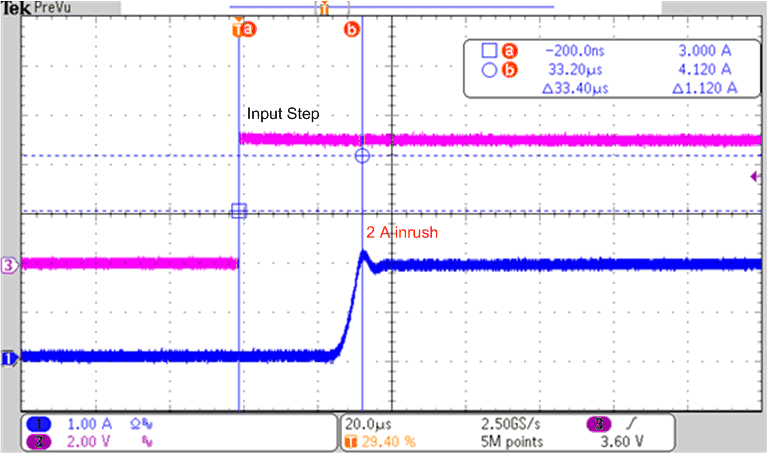
Figure 48 shows a test example of initial short-circuit inrush-current limit. Test conditions: VS = 13.5 V, input is from low to high, load is short-to-GND or with a 470-µF capacitive load, external current limit is 2 A. CH1 is the output current. CH3 is the input step.
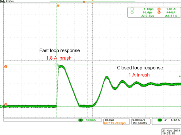
Figure 49 shows a test example of a hard short-circuit inrush-current limit. Test conditions: VS= 13.5 V, input is high, load is 5 µH + 100 mΩ, external current limit is 1 A. A short to GND suddenly happens.

 Figure 49. Hard Short-to-GND Waveform