ZHCSEX3A February   2016  – March  2016 TPS22918

PRODUCTION DATA.  

  1. 特性
  2. 应用
  3. 说明
  4. 修订历史记录
  5. Pin Configuration and Functions
  6. Specifications
    1. 6.1 Absolute Maximum Ratings
    2. 6.2 ESD Ratings
    3. 6.3 Recommended Operating Conditions
    4. 6.4 Thermal Information
    5. 6.5 Electrical Characteristics
    6. 6.6 Switching Characteristics
    7. 6.7 Typical Characteristics
      1. 6.7.1 DC Characteristics
      2. 6.7.2 AC Characteristics
  7. Parameter Measurement Information
  8. Detailed Description
    1. 8.1 Overview
    2. 8.2 Functional Block Diagram
    3. 8.3 Feature Description
      1. 8.3.1 On and Off Control
      2. 8.3.2 Quick Output Discharge (QOD)
        1. 8.3.2.1 QOD when System Power is Removed
        2. 8.3.2.2 Internal QOD Considerations
      3. 8.3.3 Adjustable Rise Time (CT)
    4. 8.4 Device Functional Modes
  9. Application and Implementation
    1. 9.1 Application Information
    2. 9.2 Typical Application
      1. 9.2.1 Design Requirements
      2. 9.2.2 Detailed Design Procedure
        1. 9.2.2.1 Input Capacitor (CIN)
        2. 9.2.2.2 Output Capacitor (CL) (Optional)
        3. 9.2.2.3 Shutdown Sequencing During Unexpected System Power Loss
        4. 9.2.2.4 VIN to VOUT Voltage Drop
        5. 9.2.2.5 Inrush Current
      3. 9.2.3 Application Curves
  10. 10Power Supply Recommendations
  11. 11Layout
    1. 11.1 Layout Guidelines
    2. 11.2 Layout Example
    3. 11.3 Thermal Considerations
  12. 12器件和文档支持
    1. 12.1 器件支持
      1. 12.1.1 开发支持
    2. 12.2 文档支持
      1. 12.2.1 相关文档 
    3. 12.3 社区资源
    4. 12.4 商标
    5. 12.5 静电放电警告
    6. 12.6 Glossary
  13. 13机械、封装和可订购信息

封装选项

机械数据 (封装 | 引脚)
散热焊盘机械数据 (封装 | 引脚)
订购信息

7 Parameter Measurement Information

TPS22918 section 81.png
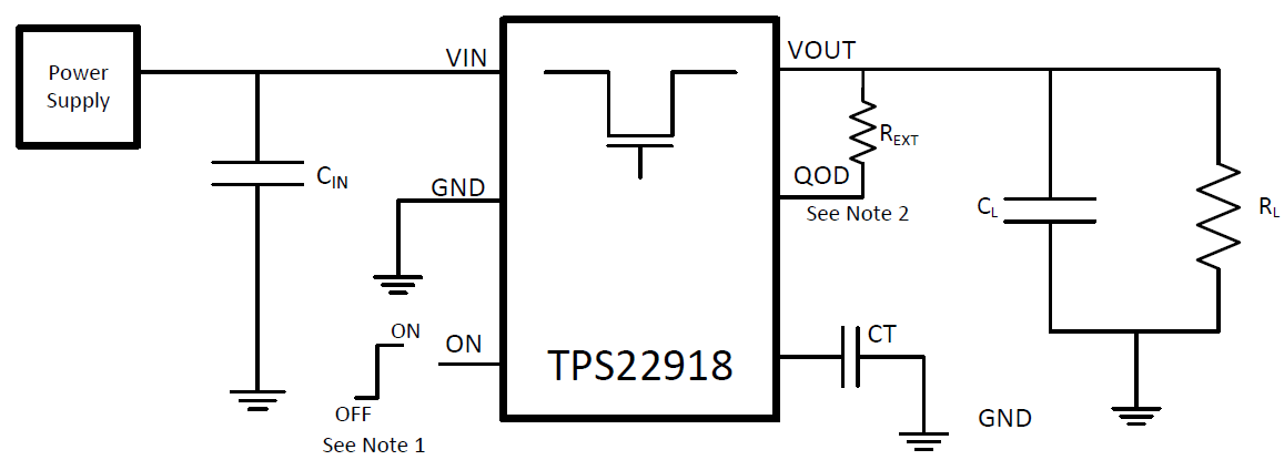
1. Rise and fall times of the control signal are 100 ns
2. Turn-off times and fall times are dependent on the time constant at the load. For TPS22918, the internal pull-down resistance RPD is enabled when the switch is disabled. The time constant is (RQOD || RL) × CL.
Figure 21. Test Circuit
TPS22918 time_wave_slvsco0.gif Figure 22. Timing Waveforms