ZHCSDD9A November 2014 – February 2015 TPS22968-Q1
PRODUCTION DATA.
- 1 特性
- 2 应用
- 3 说明
- 4 修订历史记录
- 5 Pin Configuration and Functions
-
6 Specifications
- 6.1 Absolute Maximum Ratings
- 6.2 ESD Ratings
- 6.3 Recommended Operating Conditions
- 6.4 Thermal Information
- 6.5 Electrical Characteristics (VBIAS = 5 V)
- 6.6 Electrical Characteristics (VBIAS = 3.3 V)
- 6.7 Electrical Characteristics (VBIAS = 2.5 V)
- 6.8 Switching Characteristics
- 6.9 Typical DC Characteristics
- 6.10 Typical AC Characteristics
- 7 Parameter Measurement Information
- 8 Detailed Description
- 9 Application and Implementation
- 10Power Supply Recommendations
- 11Layout
- 12器件和文档支持
- 13机械封装和可订购信息
8 Detailed Description
8.1 Overview
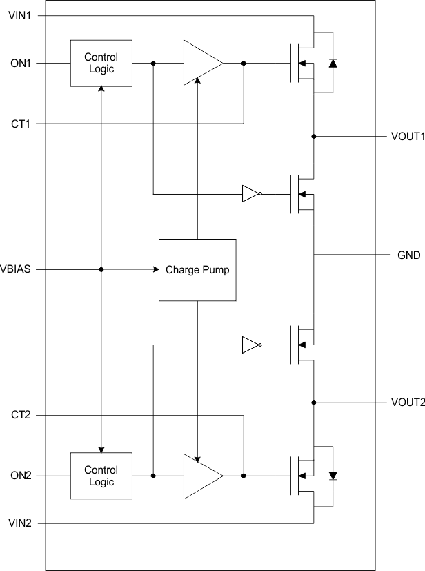
The device is a 5.5-V, 4-A, dual-channel ultra-low RON load switch with controlled turn on. The device contains two N-channel MOSFETs. Each channel can support a maximum continuous current of 4 A. Each channel is controlled by an on/off GPIO-compatible input. The ON pin must be connected and cannot be left floating. The device is designed to control the turn-on rate and therefore the inrush current. By controlling the inrush current, power supply sag can be reduced during turn-on. The slew rate for each channel is set by connecting a capacitor to GND on the CT pins.
The slew rate is proportional to the capacitor on the CT pin. Refer to Adjustable Rise Time to determine the correct CT value for a desired rise time.
The internal circuitry is powered by the VBIAS pin, which supports voltages from 2.5 to 5.5 V. This circuitry includes the charge pump, QOD, and control logic. For these internal blocks to function correctly, a voltage between 2.5 and 5.5 V must be supplied to VBIAS.
When a voltage is supplied to VBIAS and the ON1, 2 pin goes low, the QOD turns on. This connects VOUT1, 2 to GND through an on-chip resistor. The typical pulldown resistance (RPD) is 270 Ω.
8.2 Functional Block Diagram

8.3 Feature Description
8.3.1 ON/OFF Control
The ON pins control the state of the switch. Asserting ON high enables the switch. ON is active high and has a low threshold, making it capable of interfacing with low-voltage signals. The ON pin is compatible with standard GPIO logic threshold. It can be used with any microcontroller with 1.2-V or higher GPIO voltage. This pin cannot be left floating and must be tied either high or low for proper functionality.
8.3.2 Quick Output Discharge (QOD)
The TPS22968-Q1 includes a QOD feature. When the switch is disabled, a discharge resistor is connected between VOUT and GND. This resistor has a typical value of 270 Ω and prevents the output from floating while the switch is disabled.
8.3.3 Adjustable Rise Time
A capacitor to GND on the CT pins sets the slew rate for each channel. The capacitor to GND on the CT pins should be rated for 25 V and above. An approximate formula for the relationship between CT and slew rate with VBIAS = 5 V is:
where
- SR = slew rate (in µs/V)
- CT = the capacitance value on the CT pin (in pF)
- The units for the constant 25 is in µs/V.
Rise time can be calculated by multiplying the input voltage by the slew rate. Table 1 contains rise time values measured on a typical device.
Table 1. Rise Time Table
| CTx (pF) | Rise Time (µs)(1)(2) | |||||
|---|---|---|---|---|---|---|
| VIN = 5 V | VIN = 3.3 V | VIN = 2.5 V | VIN = 1.8 V | VIN = 1.2 V | VIN = 0.8 V | |
| 0 | 84 | 63 | 52 | 43 | 35 | 27 |
| 220 | 418 | 285 | 223 | 168 | 122 | 88 |
| 470 | 711 | 479 | 372 | 276 | 196 | 139 |
| 1000 | 1405 | 952 | 738 | 545 | 385 | 271 |
| 2200 | 3236 | 2174 | 1684 | 1246 | 876 | 615 |
| 4700 | 6415 | 4306 | 3317 | 2454 | 1725 | 1217 |
| 10000 | 13872 | 9261 | 7150 | 5253 | 3694 | 2591 |
8.4 Device Functional Modes
Table 2. Functional Table
| ONx | VINx to VOUTx | VOUTx to GND |
|---|---|---|
| L | Off | On |
| H | On | Off |