ZHCS791C March 2012 – July 2015 TPS2378
PRODUCTION DATA.
- 1 特性
- 2 应用
- 3 说明
- 4 修订历史记录
- 5 Pin Configuration and Functions
- 6 Specifications
-
7 Detailed Description
- 7.1 Overview
- 7.2 Functional Block Diagram
- 7.3 Feature Description
- 7.4
Device Functional Modes
- 7.4.1 PoE Overview
- 7.4.2 Threshold Voltages
- 7.4.3 PoE Start-up Sequence
- 7.4.4 Detection
- 7.4.5 Hardware Classification
- 7.4.6 Inrush and Start-up
- 7.4.7 Maintain Power Signature
- 7.4.8 Start-up and Converter Operation
- 7.4.9 PD Hotswap Operation
- 7.4.10 Start-up and Power Management, CDB and T2P
- 7.4.11 Adapter ORing
- 7.4.12 Using DEN to Disable PoE
- 7.4.13 ORing Challenges
- 8 Application and Implementation
- 9 Power Supply Recommendations
- 10Layout
- 11器件和文档支持
- 12机械、封装和可订购信息
7 Detailed Description
7.1 Overview
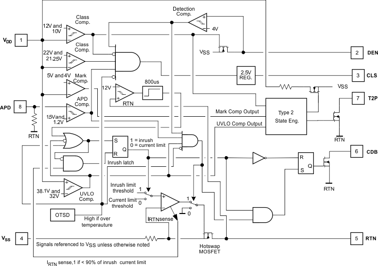
The TPS2378 device is an 8-pin integrated circuit that contains all of the features needed to implement an IEEE802.3at type-2 powered device (PD) such as Detection, Classification, Type 2 Hardware Classification, and 140-mA inrush current limit during start-up.
The TPS2378 integrates a low 0.5-Ω internal switch to allow for up to 0.85 A of continuous current through the PD during normal operation.
The TPS2378 features an auxiliary power detect (APD) input, providing priority for an external power adapter.
The TPS2378 contains several protection features such as thermal shutdown, current limit foldback, and a robust 100-V internal switch.
7.2 Functional Block Diagram
7.3 Feature Description
7.3.1 APD Auxiliary Power Detect
The APD pin is used in applications that may draw power either from the Ethernet cable or from an auxiliary power source. A voltage of more than about 1.5 V on the APD pin relative to RTN turns off the internal pass MOSFET, disables the CLS output, and enables the T2P output, giving adapter source priority over the PoE. A resistor divider (RAPD1–RAPD2 in Figure 24) provides system-level ESD protection for the APD pin, discharges leakage from the blocking diode (DA in Figure 24) and provides input voltage supervision to ensure that switch-over to the auxiliary voltage source does not occur at excessively low voltages. If not used, connect APD to RTN.
7.3.2 CDB Converter Disable Bar Pin Interface
CDB is an active low output that is pulled to RTN when the device is in inrush current limiting. It remains in a high impedance state at all other times. This pin is an open-drain output, and it may require a pullup resistor or other interface to the downstream load. CDB may be left open if it is not used.
The CDB pin can be used to inhibit downstream converter start-up by keeping the soft start pin low. Figure 15 shows an example where CDB connects to the SS pin of a UCC2897A DC-DC controller. Because CDB is an open drain output, it will not affect the soft start capacitor charge time when it deasserts. Another common use of the CDB pin is to enable a converter with an active-high enable input. In this case, CDB may require a pullup resistor to either VDD, or to a bias supply, depending on the requirements of the controller enable pin.
 Figure 15. CDB Interface
7.3.3 CLS Classification
An external resistor (RCLS in Figure 24) connected between the CLS pin and VSS provides a classification signature to the PSE. The controller places a voltage of approximately 2.5 V across the external resistor whenever the voltage differential between VDD and VSS lies from about 10.9 V to 22 V. The current drawn by this resistor, combined with the internal current drain of the controller and any leakage through the internal pass MOSFET, creates the classification current. Table 1 lists the external resistor values required for each of the PD power ranges defined by IEEE802.3at. The maximum average power drawn by the PD, plus the power supplied to the downstream load, should not exceed the maximum power indicated in Table 1. Holding APD high disables the classification signature.
High-power PSEs may perform two classification cycles if Class 4 is presented on the first cycle.
Table 1. Class Resistor Selection
| CLASS | MINIMUM POWER AT PD (W) | MAXIMUM POWER AT PD (W) | RESISTOR (Ω) |
|---|---|---|---|
| 0 | 0.44 | 12.95 | 1270 |
| 1 | 0.44 | 3.84 | 243 |
| 2 | 3.84 | 6.49 | 137 |
| 3 | 6.49 | 12.95 | 90.9 |
| 4 | 12.95 | 25.5 | 63.4 |
7.3.4 DEN Detection and Enable
DEN pin implements two separate functions. A resistor (RDEN in Figure 24) connected between VDD and DEN generates a detection signature whenever the voltage differential between VDD and VSS lies from approximately 1.4 to 10.9 V. Beyond this range, the controller disconnects this resistor to save power. The IEEE 802.3at standard specifies a detection signature resistance, RDEN from 23.75 kΩ to 26.25 kΩ, or 25 kΩ ± 5%. TI recommends a resistor of 24.9 kΩ ± 1% for RDEN.
If the resistance connected between VDD and DEN is divided into two roughly equal portions, then the application circuit can disable the PD by grounding the tap point between the two resistances. This action simultaneously spoils the detection signature and thereby signals the PSE that the PD no longer requires power.
7.3.5 Internal Pass MOSFET
RTN pin provides the negative power return path for the load. Once VDD exceeds the UVLO threshold, the internal pass MOSFET pulls RTN to VSS. Inrush limiting prevents the RTN current from exceeding about 140 mA until the bulk capacitance (CBULK in Figure 24) is fully charged. Inrush ends when the RTN current drops below about 125 mA. The RTN current is subsequently limited to about 1 A. The CDB pulls low to signal the downstream load that the bulk capacitance is fully charged. If RTN ever exceeds about 12 V for longer than 800 μs, then the TPS2378 returns to inrush limiting.
7.3.6 T2P Type-2 PSE Indicator
The TPS2378 pulls T2P to RTN whenever type-2 hardware classification has been observed or the APD pin is pulled high. The T2P output will return to a high-impedance state if the part enters thermal shutdown, the pass MOSFET enters inrush limiting, or if a type-2 PSE was not detected and the voltage on APD drops below its threshold. The circuitry that watches for type-2 hardware classification latches its result when the VDD-to-VSS voltage differential rises above the upper classification threshold. This circuit resets when the VDD-to-VSS voltage differential drops below the mark threshold. The T2P pin can be left unconnected if it is not used.
The T2P pin is an active-low, open-drain output, which indicates that a high power source is available. An optocoupler can interface the T2P pin to circuitry on the secondary side of the converter. A high-gain optocoupler and a high-impedance (for example, CMOS) receiver are recommended. Design of the T2P optocoupler interface can be accomplished as follows:
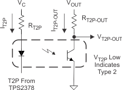 Figure 16. T2P Interface
- As shown in Figure 16, let VC = 12 V, VOUT = 5 V, RT2P–OUT = 10 kΩ, VT2P = 260 mV, VT2P = 400 mV.
- The optocoupler current transfer ratio, CTR, is needed to determine RT2P. A device with a minimum CTR of 100% at 1 mA LED bias current, IT2P, is selected. In practice, CTR will vary with temperature, LED bias current, and aging, These variations may require some iteration using the CTR-versus-IDIODE curve on the optocoupler data sheet.
- The approximate forward voltage of the optocoupler diode, VFWLED, is 1.1 V from the data sheet.
- Use Equation 2.
- Select a 10.7-kΩ resistor.
Equation 2.

7.3.7 VDD Supply Voltage
VDD pin connects to the positive side of the input supply. It provides operating power to the PD controller and allows monitoring of the input line voltage.
7.3.8 VSS
VSS pin is the input supply negative rail that serves as a local ground. The PowerPAD must be connected to this pin to ensure proper operation.
7.3.9 PowerPAD
The PowerPAD is internally connected to VSS. It should be tied to a large VSS copper area on the PCB to provide a low resistance thermal path to the circuit board. TI recommends maintaining a clearance of 0.025” between VSS and high-voltage signals such as VDD.
7.3.10 Forced, Four-Pair, High Power PoE
TPS2378 can be arranged in a dual fashion to support high power, four pair operation at 51 W at the input RJ45 connector. Additional information is available in the Dual TPS2378 PD for 51 W High Power-Four Pair PoE (SLVA625) application report.
7.4 Device Functional Modes
7.4.1 PoE Overview
The following text is intended as an aid in understanding the operation of the TPS2378 but not as a substitute for the IEEE 802.3at standard. The IEEE 802.3at standard is an update to IEEE 802.3-2008 clause 33 (PoE), adding high-power options and enhanced classification. Generally speaking, a device compliant to IEEE 802.3-2008 is referred to as a type 1 device, and devices with high power and enhanced classification will be referred to as type 2 devices. Standards change and should always be referenced when making design decisions.
The IEEE 802.3at standard defines a method of safely powering a PD (powered device) over a cable by power sourcing equipment (PSE), and then removing power if a PD is disconnected. The process proceeds through an idle state and three operational states of detection, classification, and operation. The PSE leaves the cable unpowered (idle state) while it periodically looks to see if something has been plugged in; this is referred to as detection. The low power levels used during detection are unlikely to damage devices not designed for PoE. If a valid PD signature is present, the PSE may inquire how much power the PD requires; this is referred to as classification. The PSE may then power the PD if it has adequate capacity.
Type 2 PSEs are required to do type 1 hardware classification plus a (new) data-layer classification, or an enhanced type 2 hardware classification. Type 1 PSEs are not required to do hardware or data link layer (DLL) classification. A type 2 PD must do type 2 hardware classification as well as DLL classification. The PD may return the default, 13-W current-encoded class, or one of four other choices. DLL classification occurs after power-on and the Ethernet data link has been established.
Once started, the PD must present a maintain power signature (MPS) to assure the PSE that it is still present. The PSE monitors its output for a valid MPS, and turns the port off if it loses the MPS. Loss of the MPS returns the PSE to the idle state. Figure 17 shows the operational states as a function of PD input voltage. The upper half is for IEEE 802.3-2008, and the lower half shows specific differences for IEEE 802.3at. The dashed lines in the lower half indicate these are the same (for example, Detect and Class) for both.
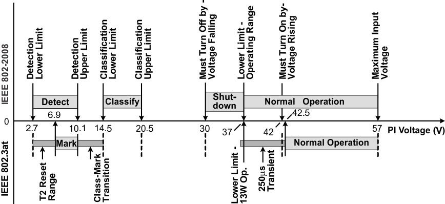 Figure 17. Threshold Voltages
The PD input, typically an RJ-45 eight-lead connector, is referred to as the power interface (PI). PD input requirements differ from PSE output requirements to account for voltage drops and operating margin. The standard allots the maximum loss to the cable regardless of the actual installation to simplify implementation. IEEE 802.3-2008 was designed to run over infrastructure including ISO/IEC 11801 class C (CAT3 per TIA/EIA-568) that may have had AWG 26 conductors. IEEE 802.3at type 2 cabling power loss allotments and voltage drops have been adjusted for 12.5-Ω power loops per ISO/IEC11801 class D (CAT5 or higher per TIA/EIA-568, typically AWG 24 conductors). Table 2 shows key operational limits broken out for the two revisions of the standard.
Table 2. Comparison of Operational Limits
| STANDARD | POWER LOOP RESISTANCE (MAX) |
PSE OUTPUT POWER (MIN) |
PSE STATIC OUTPUT VOLTAGE (MIN) |
PD INPUT POWER (MAX) |
STATIC PD INPUT VOLTAGE | |
|---|---|---|---|---|---|---|
| POWER ≤ 13 W | POWER > 13 W | |||||
| IEEE802.3at-2008 802.3at (Type 1) |
20 Ω | 15.4 W | 44 V | 13 W | 37 V – 57 V | N/A |
| 802.3at (Type 2) | 12.5 Ω | 30 W | 50 V | 25.5 W | 37 V – 57 V | 42.5 V – 57 V |
The PSE can apply voltage either between the RX and TX pairs (pins 1–2 and 3–6 for 10baseT or 100baseT), or between the two spare pairs (4–5 and 7–8). Power application to the same pin combinations in 1000baseT systems is recognized in IEEE 802.3at. 1000baseT systems can handle data on all pairs, eliminating the spare pair terminology. The PSE may only apply voltage to one set of pairs at a time. The PD uses input diode bridges to accept power from any of the possible PSE configurations. The voltage drops associated with the input bridges create a difference between the standard limits at the PI and the TPS2378 specifications.
A compliant type 2 PD has power management requirements not present with a type 1 PD. These requirements include the following:
- Must interpret type 2 hardware classification.
- Must present hardware class 4.
- Must implement DLL negotiation.
- Must behave like a type 1 PD during inrush and start-up.
- Must not draw more than 13 W for 80 ms after the PSE applies operating voltage (power up).
- Must not draw more than 13 W if it has not received a type 2 hardware classification or received permission through DLL.
- Must meet various operating and transient templates.
- Optionally monitor for the presence or absence of an adapter (assume high power).
As a result of these requirements, the PD must be able to dynamically control its loading, and monitor T2P for changes. In cases where the design needs to know specifically if an adapter is plugged in and operational, the adapter should be individually monitored, typically with an optocoupler.
7.4.2 Threshold Voltages
The TPS2378 has a number of internal comparators with hysteresis for stable switching between the various states. Figure 18 relates the parameters in Electrical Characteristics to the PoE states. The mode labeled Idle between Classification and Operation implies that the DEN, CLS, and RTN pins are all high impedance. The state labeled Mark, which is drawn in dashed lines, is part of the new type 2 hardware class state machine.
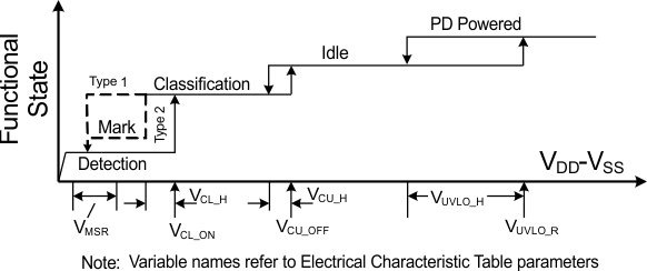 Figure 18. Threshold Voltages
7.4.3 PoE Start-up Sequence
The waveforms of Figure 19 demonstrate detection, classification, and start-up from a PSE with type 2 hardware classification. The key waveforms shown are V(VDD-VSS), V(RTN-VSS), and IPI. IEEE 802.3at requires a minimum of two detection levels, two class and mark cycles, and start-up from the second mark event. VRTN to VSS falls as the TPS2378 charges CBULK following application of full voltage. In Figure 19, deassertion of the CDB signal is delayed and used to enable load current as seen in the IPI waveform.
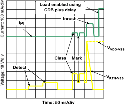 Figure 19. Start-up
7.4.4 Detection
The TPS2378 pulls DEN to VSS whenever V(VDD-VSS) is below the lower classification threshold. When the input voltage rises above VCL_ON, the DEN pin goes to an open-drain condition to conserve power. While in detection, RTN is high impedance, and almost all the internal circuits are disabled. An RDEN of 24.9 kΩ (±1%), presents the correct signature. It may be a small, low-power resistor because it only sees a stress of about 5 mW. A valid PD detection signature is an incremental resistance ( ΔV / ΔI ) from 23.7 kΩ to 26.3 kΩ at the PI.
The detection resistance seen by the PSE at the PI is the result of the input bridge resistance in series with the parallel combination of RDEN and internal VDD loading. The input diode bridge’s incremental resistance may be hundreds of Ω at the low currents drawn when 2.7 V is applied to the PI. The input bridge resistance is partially compensated by the TPS2378 effective resistance during detection.
The type 2 hardware classification protocol of IEEE 802.3at specifies that a type 2 PSE drops its output voltage into the detection range during the classification sequence. The PD is required to have an incorrect detection signature in this condition, which is referred to as a mark event (see Figure 19). After the first mark event, the TPS2378 will present a signature less than 12 kΩ until it has experienced a V(VDD-VSS) voltage below the mark reset threshold (VMSR). This is explained more fully under Hardware Classification.
7.4.5 Hardware Classification
Hardware classification allows a PSE to determine a PD’s power requirements before powering, and helps with power management once power is applied. Type 2 hardware classification permits high power PSEs and PDs to determine whether the connected device can support high-power operation. A type 2 PD presents class 4 in hardware to indicate that it is a high-power device. A type 1 PSE will treat a class 4 device like a class 0 device, allotting 13 W if it chooses to power the PD. A PD that receives a 2-event class understands that it is powered from a high-power PSE and it may draw up to 25.5 W immediately after the 80-ms start-up period completes. A type 2 PD that does not receive a 2-event hardware classification may choose to not start, or must start in a 13-W condition and request more power through the DLL after start-up. The standard requires a type 2 PD to indicate that it is underpowered if this occurs. Start-up of a high-power PD under 13 W implicitly requires some form of powering down sections of the application circuits.
The maximum power entries in Table 1 determine the class the PD must advertise. The PSE may disconnect a PD if it draws more than its stated class power, which may be the hardware class or a lower DLL-derived power level. The standard permits the PD to draw limited current peaks that increase the instantaneous power above the Table 1 limit; however, the average power requirement always applies.
The TPS2378 implements two-event classification. Selecting an RCLS of 63.4 Ω provides a valid type 2 signature. TPS2378 may be used as a compatible type 1 device simply by programming class 0–3 per Table 1. DLL communication is implemented by the Ethernet communication system in the PD and is not implemented by the TPS2378.
The TPS2378 disables classification above VCU_ON to avoid excessive power dissipation. CLS voltage is turned off during PD thermal limiting or when APD or DEN is active. The CLS output is inherently current-limited, but should not be shorted to VSS for long periods of time.
Figure 20 shows how classification works for the TPS2378. Transition from state-to-state occurs when comparator thresholds are crossed (see Figure 17 and Figure 18). These comparators have hysteresis, which adds inherent memory to the machine. Operation begins at idle (unpowered by PSE) and proceeds with increasing voltage from left to right. A 2-event classification follows the (heavy lined) path towards the bottom, ending up with a latched type 2 decode along the lower branch that is highlighted. This state results in a low T2P during normal operation. Once the valid path to type 2 PSE detection is broken, the input voltage must transition below the mark reset threshold to start anew.
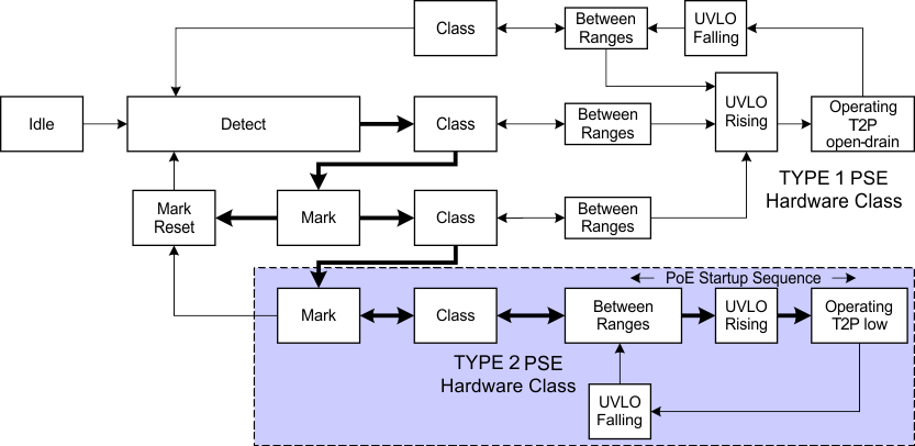 Figure 20. Two-Event Class Internal States
7.4.6 Inrush and Start-up
IEEE 802.3at has a start-up current and time limitation, providing type 2 PSE compatibility for type 1 PDs. A type 2 PSE limits output current to from 400 mA to 450 mA for up to 75 ms after power up (applying 48 V to the PI) to mirror type 1 PSE functionality. The type 2 PSE will support higher output current after 75 ms. The TPS2378 implements a 140-mA inrush current, which is compatible with all PSE types. A high-power PD must limit its converter start-up peak current. The operational current cannot exceed 400 mA for a period of 80 ms or longer. This requirement implicitly requires some form of powering down sections of the application circuits.
7.4.7 Maintain Power Signature
The MPS is an electrical signature presented by the PD to assure the PSE that it is still present after operating voltage is applied. A valid MPS consists of a minimum dc current of 10 mA (or a 10-mA pulsed current for at least 75 ms every 325 ms) and an AC impedance lower than 26.3 kΩ in parallel with 0.05 μF. The AC impedance is usually accomplished by the minimum operating CBULK requirement of 5 μF. When either APD or DEN is used to force the hotswap switch off, the DC MPS will not be met. A PSE that monitors the DC MPS will remove power from the PD when this occurs. A PSE that monitors only the ac MPS may remove power from the PD.
7.4.8 Start-up and Converter Operation
The internal PoE UVLO (Undervoltage Lock Out) circuit holds the hotswap switch off before the PSE provides full voltage to the PD. This prevents the downstream converter circuits from loading the PoE input during detection and classification. The converter circuits will discharge CBULK while the PD is unpowered. Thus V(VDD-RTN) will be a small voltage just after full voltage is applied to the PD, as seen in Figure 19. The PSE drives the PI voltage to the operating range once it has decided to power up the PD. When VVDD rises above the UVLO turn-on threshold (VUVLO_R, approximately 38 V) with RTN high, the TPS2378 enables the hotswap MOSFET with a approximately 140 mA (inrush) current limit as seen in Figure 21. The CDB pin is active while CBULK charges and VRTN falls from VVDD to nearly VVSS. Additional loading applied between VVDD and VRTN during the inrush state may prevent successful PD and subsequent converter start up. Once the inrush current falls about 10% below the inrush current limit, the PD current limit switches to the operational level (approximately 1000 mA) and CDB is deassert to allow downstream converter circuitry to start. In Figure 21, T2P is active when a type 2 PSE is plugged in.
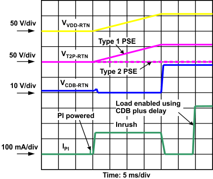 Figure 21. Power Up and Start
7.4.9 PD Hotswap Operation
IEEE 802.3at has taken a new approach to PSE output limiting. A type 2 PSE must meet an output current vs time template with specified minimum and maximum sourcing boundaries. The peak output current may be as high as 50 A for 10 μs or 1.75 A for 75 ms. This makes robust protection of the PD device even more important than it was in IEEE 802.3-2008.
The internal hotswap MOSFET is protected against output faults and input voltage steps with a current limit and deglitched (time-delay filtered) foldback. An overload on the pass MOSFET engages the current limit, with V(RTN-VSS) rising as a result. If V(RTN-VSS) rises above approximately 12 V for longer than approximately 800 μs, the current limit reverts to the inrush value. The 800-μs deglitch feature prevents momentary transients from causing a PD reset, provided that recovery lies within the bounds of the hotswap and PSE protection. Figure 22 shows an example of the RTN current profile during VDD to RTN short circuit. The hotswap MOSFET goes into current limit, causing the RTN voltage to increase. Once VRTN exceeds 12 V, IRTN, which was clamped to the current limit drops to the level of inrush current limit after 800 µs. The inrush current limit is reestablished when V(VDD-VSS) drops below UVLO.
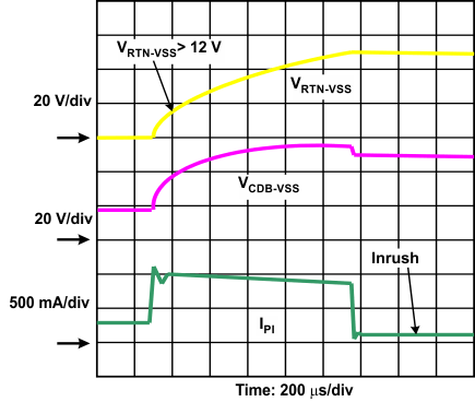 Figure 22. Response to PD Output Short Circuit
The PD control has a thermal sensor that protects the internal hotswap MOSFET. Conditions like start-up or operation into a VDD-to-RTN short cause high power dissipation in the MOSFET. An over-temperature shutdown (OTSD) turns off the hotswap MOSFET and class regulator, which are restarted after the device cools. The hotswap MOSFET will be re-enabled with the inrush current limit when exiting from an overtemperature event. Pulling DEN to VSS during powered operation causes the internal hotswap MOSFET to turn off. This feature allows a PD with option three ORing per Figure 23 to achieve adapter priority.
The hotswap switch will be forced off under the following conditions:
- VAPD above VAPDEN (approximately 1.5 V),
- V(DEN –VSS) < VPD-DIS when V(VDD-VSS) is in the operational range,
- PD is over-temperature, or
- V(DEN –VSS) < PoE UVLO falling threshold (approximately 32 V).
7.4.10 Start-up and Power Management, CDB and T2P
CDB (converter disable) is an active-low pin that indicates when the internal hotswap MOSFET is in inrush limiting. CDB deasserts when inrush is over and can be used to enable a downstream converter to start up. Common interfaces to the converter controller include the soft start or enable pins.
T2P (type 2 PSE) is an active-low multifunction pin that indicates if
[(PSE = Type_2) or (1.5 V < VAPD)] and (pd current limit ≠ Inrush).
The APD term allows the PD to operate from an adapter at high-power if a type 2 PSE is not present, assuming the adapter has sufficient capacity. Applications must monitor the state of T2P to detect power source transitions. Transitions could occur when a local power supply is added or dropped, or when a PSE is enabled on the far end. The PD may be required to adjust the load appropriately. The usage of T2P is demonstrated in Figure 24.
In order for a type 2 PD to operate at less than 13 W for the first 80 ms after power application, the various delays must be estimated and used by the application controller to meet the requirement. The bootup time of many application processors may be long enough to eliminate the need for any timing.
7.4.11 Adapter ORing
Many PoE-capable devices are designed to operate from either a wall adapter or PoE power. A local power solution adds cost and complexity, but allows a product to be used if PoE is not available in a particular installation. While most applications only require that the PD operate when both sources are present, the TPS2378 supports forced operation from either of the power sources. Figure 23 illustrates three options for diode ORing external power into a PD. Only one option would be used in any particular design. Option 1 applies power to the TPS2378 PoE input, option 2 applies power between the TPS2378 PoE section and the power circuit, and option 3 applies power to the output side of the converter. Each of these options has advantages and disadvantages. Many of the basic ORing configurations and much of the discussion contained in the application note Advanced Adapter ORing Solutions using the TPS23753 (SLVA306), apply to the TPS2378 incorporating a DC/DC converter.
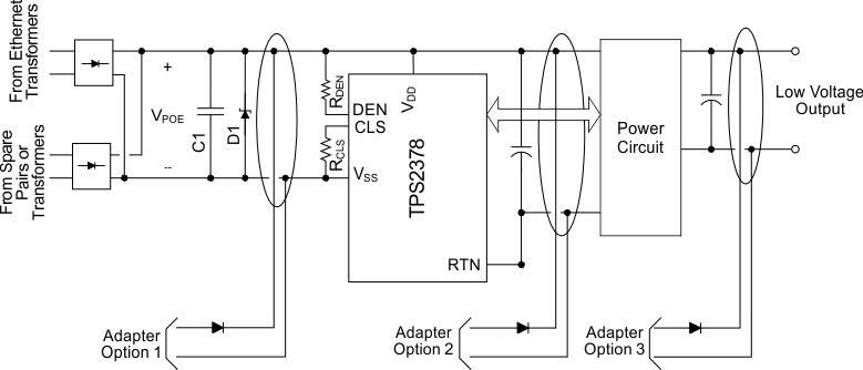 Figure 23. Oring Configurations
The IEEE standards require that the Ethernet cable be isolated from ground and all other system potentials. The adapter must meet a minimum 1500 Vac dielectric withstand test between the output and all other connections for ORing options 1 and 2. The adapter only needs this isolation for option 3 if it is not provided by the converter.
Adapter ORing diodes are shown for all the options to protect against a reverse voltage adapter, a short on the adapter input pins, or damage to a low-voltage adapter. ORing is sometimes accomplished with a MOSFET in option 3.
7.4.12 Using DEN to Disable PoE
The DEN pin may be used to turn the PoE hotswap switch off by pulling it to VSS while in the operational state, or to prevent detection when in the idle state. A low voltage on DEN forces the hotswap MOSFET off during normal operation. Additional information is available in the Advanced Adapter ORing Solutions using the TPS23753 (SLVA306) application report.
7.4.13 ORing Challenges
Preference of one power source presents a number of challenges. Combinations of adapter output voltage (nominal and tolerance), power insertion point, and which source is preferred determine solution complexity. Several factors adding to the complexity are the natural high-voltage selection of diode ORing (the simplest method of combining sources), the current limit implicit in the PSE, and PD inrush and protection circuits (necessary for operation and reliability). Creating simple and seamless solutions is difficult, if not impossible, for many of the combinations. However, the TPS2378 offers several built-in features that simplify some combinations.
Several examples demonstrate the limitations inherent in ORing solutions. Diode ORing a 48-V adapter with PoE (option 1) presents the problem that either source may have the higher voltage. A blocking switch would be required to assure that one source dominates. A second example combines a 12-V adapter with PoE using option 2. The converter draws approximately four times the current at 12 V from the adapter than it does from PoE at 48 V. Transition from PoE power to adapter may demand more current than can be supplied by the PSE. The converter must be turned off while the CBULK capacitance charges, with a subsequent converter restart at the higher voltage and lower input current. A third example involves the loss of the MPS when running from the adapter, causing the PSE to remove power from the PD. If AC power is then lost, the PD will stop operating until the PSE detects and powers the PD.