ZHCS791C March 2012 – July 2015 TPS2378
PRODUCTION DATA.
- 1 特性
- 2 应用
- 3 说明
- 4 修订历史记录
- 5 Pin Configuration and Functions
- 6 Specifications
-
7 Detailed Description
- 7.1 Overview
- 7.2 Functional Block Diagram
- 7.3 Feature Description
- 7.4
Device Functional Modes
- 7.4.1 PoE Overview
- 7.4.2 Threshold Voltages
- 7.4.3 PoE Start-up Sequence
- 7.4.4 Detection
- 7.4.5 Hardware Classification
- 7.4.6 Inrush and Start-up
- 7.4.7 Maintain Power Signature
- 7.4.8 Start-up and Converter Operation
- 7.4.9 PD Hotswap Operation
- 7.4.10 Start-up and Power Management, CDB and T2P
- 7.4.11 Adapter ORing
- 7.4.12 Using DEN to Disable PoE
- 7.4.13 ORing Challenges
- 8 Application and Implementation
- 9 Power Supply Recommendations
- 10Layout
- 11器件和文档支持
- 12机械、封装和可订购信息
8 Application and Implementation
NOTE
Information in the following applications sections is not part of the TI component specification, and TI does not warrant its accuracy or completeness. TI’s customers are responsible for determining suitability of components for their purposes. Customers should validate and test their design implementation to confirm system functionality.
8.1 Application Information
The TPS2378 has the flexibility to be implemented in IEEE802.3at and Universal Power Over Ethernet (UPOE) PDs. Therefore, it can be used in a wide range applications such as video and VoIP telephones, multiband access points, security cameras, and pico-base stations.
8.2 Typical Application
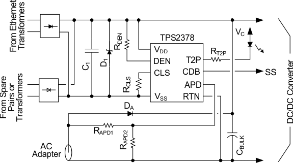
 Figure 24. Typical Application Circuit
8.2.1 Design Requirements
For this design example, use the parameters in Table 3.
Table 3. Design Parameters
| PARAMETER | TEST CONDITIONS | MIN | MAX | UNIT |
|---|---|---|---|---|
| POWER INTERFACE | ||||
| Input voltage | Applied to the power pins of connectors J1 or J3 (adapter) | 0 | 57 | V |
| Operating voltage | After start-up | 30 | 57 | V |
| Input UVLO | Rising input voltage at device terminals | — | 40 | V |
| Falling input voltage | 30.5 | — | ||
| Detection voltage | At device terminals | 1.4 | 10.1 | V |
| Classification voltage | At device terminals | 11.9 | 23 | V |
| Classification current | Class 4 | 38 | 42 | mA |
| Inrush current limit | 100 | 180 | mA | |
| Operating curent-limit | 850 | 1200 | mA | |
8.2.2 Detailed Design Requirements
8.2.2.1 Input Bridges and Schottky Diodes
Using Schottky diodes instead of PN junction diodes for the PoE input bridges will reduce the power dissipation in these devices by about 30%. There are, however, some things to consider when using them. The IEEE standard specifies a maximum backfeed voltage of 2.8 V. A 100-kΩ resistor is placed between the unpowered pairs and the voltage is measured across the resistor. Schottky diodes often have a higher reverse leakage current than PN diodes, making this a harder requirement to meet. To compensate, use conservative design for diode operating temperature, select lower-leakage devices where possible, and match leakage and temperatures by using packaged bridges.
Schottky diode leakage currents and lower dynamic resistances can impact the detection signature. Setting reasonable expectations for the temperature range over which the detection signature is accurate is the simplest solution. Increasing RDEN slightly may also help meet the requirement.
Schottky diodes have proven less robust to the stresses of ESD transients than PN junction diodes. After exposure to ESD, Schottky diodes may become shorted or leak. Take care to provide adequate protection in line with the exposure levels. This protection may be as simple as ferrite beads and capacitors.
As a general recommendation, use 1 A or 2 A, 100 V rated discrete or bridge diodes for the input rectifiers.
8.2.2.2 Protection, D1
A TVS, D1, across the rectified PoE voltage per Figure 24 must be used. TI recommends a SMAJ58A, or equivalent, is recommended for general indoor applications. If an adapter is connected from VDD to RTN, as in ORing option 2 above, then voltage transients caused by the input cable inductance ringing with the internal PD capacitance can occur. Adequate capacitive filtering or a TVS must limit this voltage to within the absolute maximum ratings. Outdoor transient levels or special applications require additional protection.
8.2.2.3 Capacitor, C1
The IEEE 802.3at standard specifies an input bypass capacitor (from VDD to VSS) of 0.05 μF to 0.12 μF. Typically a 0.1 μF, 100 V, 10% ceramic capacitor is used.
8.2.2.4 Detection Resistor, RDEN
The IEEE 802.3at standard specifies a detection signature resistance, RDEN between 23.7 kΩ and 26.3 kΩ, or 25 kΩ ± 5%. A resistor of 24.9 kΩ ± 1% is recommended for RDEN.
8.2.2.5 Classification Resistor, RCLS
Connect a resistor from CLS to VSS to program the classification current according to the IEEE 802.3at standard. The class power assigned should correspond to the maximum average power drawn by the PD during operation. Select RCLS according to Table 1.
8.2.2.6 APD Pin Divider Network RAPD1, RAPD2
For an adapter voltage threshold to switch from PoE to adapter at 37 V, choose 10 kΩ for RAPD2.


Solving for RAPD1:
8.2.3 Application Curves
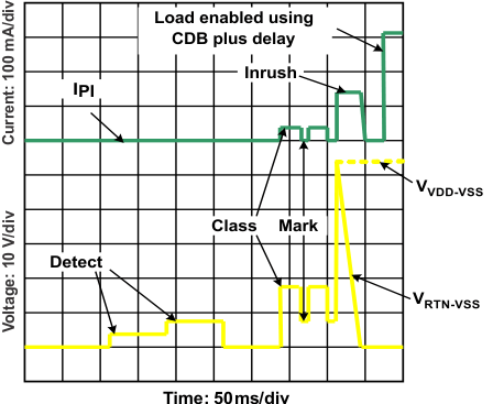
 Figure 25. Start-up
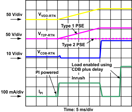
 Figure 26. Power Up and Start