ZHCS845A March 2012 – July 2015 TPS2379
PRODUCTION DATA.
- 1 特性
- 2 应用
- 3 说明
- 4 修订历史记录
- 5 Pin Configuration and Functions
- 6 Specifications
- 7 Parameter Measurement Information
-
8 Detailed Description
- 8.1 Overview
- 8.2 Functional Block Diagram
- 8.3 Feature Description
- 8.4
Device Functional Modes
- 8.4.1
PoE Overview
- 8.4.1.1 Threshold Voltages
- 8.4.1.2 PoE Start-Up Sequence
- 8.4.1.3 Detection
- 8.4.1.4 Hardware Classification
- 8.4.1.5 Inrush and Start-up
- 8.4.1.6 Maintain Power Signature
- 8.4.1.7 Start-up and Operation
- 8.4.1.8 PD Hotswap Operation
- 8.4.1.9 CDB and T2P
- 8.4.1.10 Auxiliary Pass MOSFET Control
- 8.4.1.11 Using DEN to Disable PoE
- 8.4.1
PoE Overview
- 9 Application and Implementation
- 10Power Supply Recommendations
- 11Layout
- 12器件和文档支持
- 13机械、封装和可订购信息
8 Detailed Description
8.1 Overview
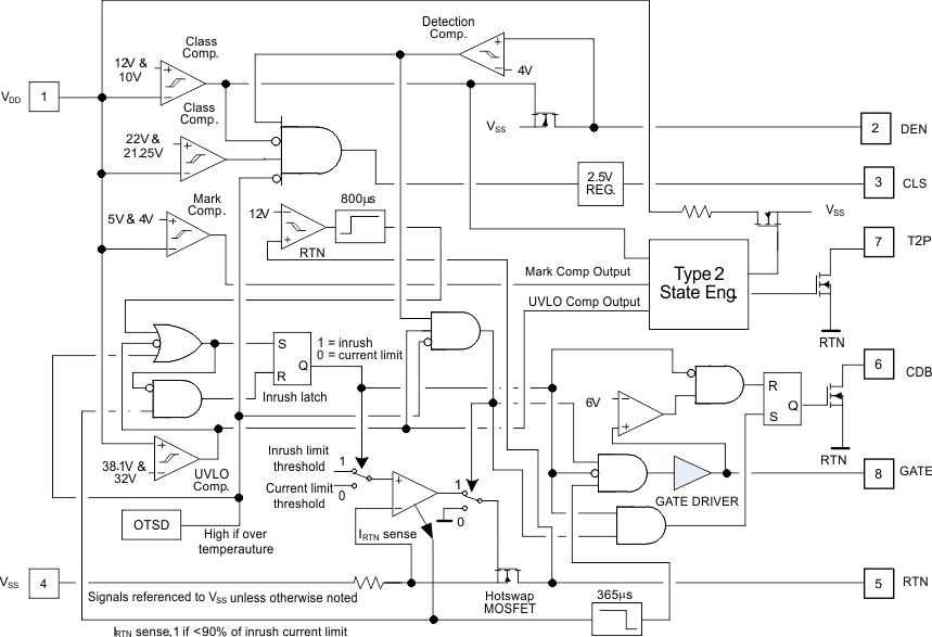
The TPS2379 device is an 8-pin integrated circuit that contains all of the features needed to implement an IEEE802.3at type-2 powered device (PD) such as Detection, Classification, Type 2 Hardware Classification, and 140mA inrush current limit during start-up.
The TPS2379 integrates a low 0.5-Ω internal switch to allow for up to 0.85 A of continuous current through the PD during normal operation.
The TPS2379 supports higher power PoE applications through the use of an external pass transistor.
The TPS2379 contains several protection features such as thermal shutdown, current limit foldback, and a robust 100V internal switch.
8.2 Functional Block Diagram
8.3 Feature Description
8.3.1 CDB Converter Disable Bar Pin Interface
CDB is an active low output that is pulled to RTN when the device is in inrush current limiting, going open when the inrush period has completed once the GATE output has become higher than 6 V. This ensures the external pass transistor is enhanced before the load is enabled. It remains in a high impedance state at all other times. This pin is an opendrain output and may require a pullup resistor or other interface to the downstream load. CDB may be left open if unused.
The CDB pin can inhibit downstream converter start up by keeping the soft start pin low. Figure 16 shows where the CDB connects to the SS pin of a UCC2897A DC-DC controller. Because CDB is an open drain output, it will not affect the soft start capacitor charge time when it deasserts. The CDB pin can also enable a converter with an active-high enable input. In this case, CDB may require a pullup resistor to either VDD, or to a bias supply, depending on the requirements of the controller enable pin.
 Figure 16. CDB Interface
8.3.2 CLS Classification
An external resistor (RCLS) connected between the CLS pin and VSS provides a classification signature to the PSE. The controller places a voltage of approximately 2.5 V across the external resistor whenever the voltage differential between VDD and VSS is between about 10.9 V and 22 V. The current drawn by this resistor, combined with the internal current drain of the controller and any leakage through the internal pass MOSFET, creates the classification current. Table 1 lists the external resistor values required for each of the PD power ranges defined by IEEE802.3at. The maximum average power drawn by the PD combined with the power supplied to the downstream load should not exceed the maximum power indicated in Table 1.
Table 1. Class Resistor Selection
| CLASS | MINIMUM POWER AT PD (W) | MAXIMUM POWER AT PD | RESISTOR RCLS (Ω) |
|---|---|---|---|
| 0 | 0.44 | 12.95 | 1270 |
| 1 | 0.44 | 3.84 | 243 |
| 2 | 3.84 | 6.49 | 137 |
| 3 | 6.49 | 12.95 | 90.9 |
| 4 | 12.95 | 25.5 | 63.4 |
8.3.3 DEN Detection and Enable
DEN pin implements two separate functions. A resistor (RDEN) connected between VDD and DEN generates a detection signature whenever the voltage differential between VDD and VSS is from 1.4 V and 10.9 V. Beyond this range, the controller disconnects this resistor to save power. The IEEE 802.3at standard specifies a detection signature resistance, RDEN from 23.75 kΩ to 26.25 kΩ, or 25 kΩ ± 5%. A resistor of 24.9 kΩ ± 1% is recommended for RDEN.
If the resistance connected between VDD and DEN is divided into two roughly equal portions, then the application circuit can disable the PD by grounding the tap point between the two resistances. This action simultaneously spoils the detection signature and thereby signals the PSE that the PD no longer requires power.
8.3.4 GATE Auxiliary Gate Driver
GATE pin allows the connection of an external pass MOSFET in parallel with the internal pass transistor. The GATE pin enables the external transistor after inrush has completed. The current is divided between the external MOSFET and the internal transistor as a function of their respective resistances. The addition of a balancing resistor (RBLST) in series with RTN and the external MOSFET can ensure the desired distribution of the two currents. When the RTN current exceeds the current limit threshold, the GATE pin will pull low after a 365 μs delay. The GATE pin is pulled low in thermal shutdown. After the controller cools down and the inrush cycle is complete, the GATE pin rises again.
A nonstandard PoE system can be designed to meet extended power requirements and retain the PoE benefits, such as protection of non-PoE devices and fault tolerance. This type of solution will not comply with IEEE802.3at and should be designed and operated as stand-alone system. The TPS2379 GATE pin controls an external pass MOSFET as shown in Figure 17. When the inrush is complete, GATE sources 38 μA to enable Q1, the external pass MOSFET. When Q1 is fully enhanced, CDB deasserts and enables the load. Delaying the deassertion of CDB until Q1 becomes fully enhanced prevents nuisance overcurrent faults that could occur with heavy start-up loads. A resistor from GATE to VSS is not required to ensure that Q1 turns off. If a resistor from GATE to VSS is used, choose a value large enough so that the GATE sourcing current can fully enhance Q1.
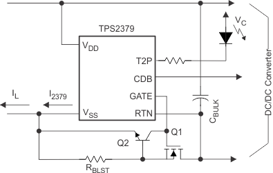 Figure 17. GATE Interface
8.3.4.1 External Boost Circuit (Q1, Q2, and RBLST) Considerations
The IEEE802.3at template bounds the peak PSE output current from 50 A for 10 μs and 1.75 A for 75 ms for a two-pair system. In a nonstandard, four-pair system, these current levels may double. During an overload event, the TPS2379 device will limit current to approximately 1 A and the rest of the current will flow through Q1 and RBLST. Ignoring the ballast resistor and parasitic impedances, the current through Q1 could be as high as 99 A.
Actual system level behavior will be influenced by the circuit parasitic impedances, diode bridge impedance, contact resistances, external MOSFET resistance, and input voltage droop during the overload event. The impedances act to reduce the peak current as well as drop the voltage across Q1 during the overload event. Evaluate the overload performance of your system and ensure that the selected external MOSFET safe operating area (SOA) is not violated during the output overload. The duration of the overload can be terminated if the input voltage droop to the TPS2379 goes below the UVLO falling threshold (typically 32 V). When UVLO occurs, the internal MOSFET is disabled, GATE goes low and the external MOSFET is disabled. This shortened overload duration is beneficial when evaluating the external MOSFET SOA performance.
Additional limiting and control of the external output overload current can be achieved by using the ballast resistor, RBLST. RBLST helps balance the internal and external MOSFET load currents and implements external current limiting through Q2. The load current, IL, divides between the external Q1 and the internal pass MOSFET of the TPS2379 as shown Equation 1.

RQ1 is the ON resistance of Q1 and R2379 is the ON resistance of the TPS2379. Q2 can be used to force Q1 to limit its current when the voltage across RBLST exceeds VBEON of Q2. For further discussion of these details and additional considerations involving PD classification, see the application report titled Implementing a 60-W End-to-End PoE System (SLVA498).
8.3.5 Internal Pass MOSFET
RTN pin provides the negative power return path for the load. When VDD exceeds the UVLO threshold, the internal pass MOSFET pulls RTN to VSS. Inrush limiting prevents the RTN current from exceeding 140 mA until the bulk capacitance (CBULK in Figure 26) is fully charged. Inrush ends when the RTN current drops below about 125 mA. The RTN current is subsequently limited to about 1 A. CDB pulls low to signal the downstream load that the bulk capacitance is fully charged. If RTN ever exceeds about 12 V for longer than 800 μs, the TPS2379 returns to inrush limiting.
8.3.6 T2P Type-2 PSE Indicator
The TPS2379 pulls T2P to RTN when type-2 hardware classification has been observed. The T2P output will return to a high-impedance state if the part enters thermal shutdown, the pass MOSFET enters inrush limiting, or if a type-2 PSE was not detected. The circuitry that watches for type-2 hardware classification latches its result when the VDD-to-VSS voltage differential rises above the upper classification threshold. This circuit resets when the VDD-to-VSS voltage differential drops below the mark threshold. The T2P pin can be left unconnected if unused.
The T2P pin is an active-low, opendrain output which indicates that a high power source is available. An optocoupler can interface the T2P pin to circuitry on the secondary side of the converter. A high-gain optocoupler and a high-impedance (that is, CMOS) receiver are recommended. Figure 18 presents the design of the T2P optocoupler interface.
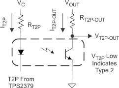 Figure 18. T2P Interface
To design the T2P octocoupler interface, do the following:
- Let VC = 12 V, VOUT = 5 V, RT2P-OUT = 10 kΩ, VT2P = 260 mV, VT2P-OUT = 400 mV.
- The optocoupler current transfer ratio, CTR, will be needed to determine RT2P. A device with a minimum CTR of 100% at 1 mA LED bias current, IT2P, is selected. CTR will vary with temperature, LED bias current, and aging. These variations may require some iteration using the CTR-versus-IDIODE curve on the optocoupler data sheet.
- The approximate forward voltage of the optocoupler diode, VFWLED, is 1.1 V from the data sheet.
- Select a 10.7-kΩ resistor.
- Select a 10.7-kΩ resistor.
Equation 3.

8.3.7 VDD Supply Voltage
VDD pin connects to the positive side of the input supply. It provides operating power to the PD controller and allows monitoring of the input line voltage.
8.3.8 VSS
VSS pin is the input supply negative rail that serves as a local ground. The PowerPAD must be connected to this pin to ensure proper operation.
8.4 Device Functional Modes
8.4.1 PoE Overview
The following text is intended as an aid in understanding the operation of the TPS2379 but not as a substitute for the IEEE 802.3at standard. The IEEE 802.3at standard is an update to IEEE 802.3-2008 clause 33 (PoE), adding high-power options and enhanced classification. Generally speaking, a device compliant to IEEE 802.3-2008 is referred to as a type 1 device, and devices with high power and enhanced classification will be referred to as type 2 devices. Standards change and should always be referenced when making design decisions.
The IEEE 802.3at standard defines a method of safely powering a PD (powered device) over a cable by power sourcing equipment (PSE), and then removing power if a PD is disconnected. The process proceeds through an idle state and three operational states of detection, classification, and operation. The PSE leaves the cable unpowered (idle state) while it periodically looks to see if something has been plugged in; this is referred to as detection. The low power levels used during detection are unlikely to damage devices not designed for PoE. If a valid PD signature is present, the PSE may inquire how much power the PD requires; this is referred to as classification. The PSE may then power the PD if it has adequate capacity.
Type 2 PSEs are required to do type 1 hardware classification plus a (new) data-layer classification, or an enhanced type 2 hardware classification. Type 1 PSEs are not required to do hardware or data link layer (DLL) classification. A type 2 PD must do type 2 hardware classification as well as DLL classification. The PD may return the default, 13W current-encoded class, or one of four other choices. DLL classification occurs after power-on and the Ethernet data link has been established.
When started, the PD must present a maintain power signature (MPS) to assure the PSE that it is still present. The PSE monitors its output for a valid MPS, and turns the port off if it loses the MPS. Loss of the MPS returns the PSE to the idle state. Figure 19 shows the operational states as a function of PD input voltage. The upper half is for IEEE 802.3-2008, and the lower half shows specific differences for IEEE 802.3at. The dashed lines in the lower half indicate these are the same (that is, Detect and Class) for both.
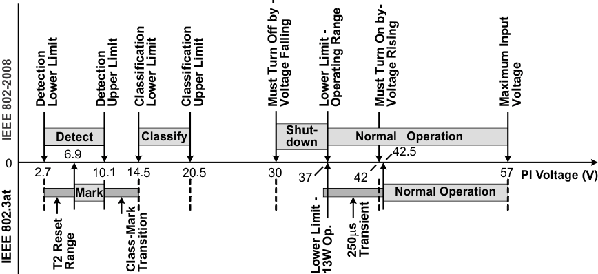 Figure 19. Threshold Voltages
The PD input, typically an RJ-45 eight-lead connector, is referred to as the power interface (PI). PD input requirements differ from PSE output requirements to account for voltage drops and operating margin. The standard allots the maximum loss to the cable regardless of the actual installation to simplify implementation. IEEE 802.3-2008 was designed to run over infrastructure including ISO/IEC 11801 class C (CAT3 per TIA/EIA-568) that may have had AWG 26 conductors. IEEE 802.3at type 2 cabling power loss allotments and voltage drops have been adjusted for 12.5 Ω power loops per ISO/IEC11801 class D (CAT5 or higher per TIA/EIA-568, typically AWG #24 conductors). Table 2 shows key operational limits broken out for the two revisions of the standard.
Table 2. Comparison of Operational Limits
| STANDARD | POWER LOOP RESISTANCE (max) |
PSE OUTPUT POWER (min) |
PSE STATIC OUTPUT VOLTAGE (min) |
PD INPUT POWER (max) |
STATIC PD INPUT VOLTAGE | |
|---|---|---|---|---|---|---|
| Power ≤12.95W | Power >12.95W | |||||
| IEEE802.3at-2008 802.3at (Type 1) |
20Ω | 15.4W | 44V | 12.95W | 37V – 57V | N/A |
| 802.3at (Type 2) | 12.5Ω | 30W | 50V | 25.5W | 37V – 57V | 42.5V – 57V |
The PSE can apply voltage either between the RX and TX pairs (pins 1 - 2 and 3 - 6 for 10baseT or 100baseT), or between the two spare pairs (4 - 5 and 7 - 8). Power application to the same pin combinations in 1000baseT systems is recognized in IEEE 802.3at. 1000baseT systems can handle data on all pairs, eliminating the spare pair terminology. The PSE may only apply voltage to one set of pairs at a time. The PD uses input diode bridges to accept power from any of the possible PSE configurations. The voltage drops associated with the input bridges create a difference between the standard limits at the PI and the TPS2379 specifications.
A compliant type 2 PD has power management requirements not present with a type 1 PD. These requirements include the following:
- Must interpret type 2 hardware classification,
- Must present hardware class 4,
- Must implement DLL negotiation,
- Must behave like a type 1 PD during inrush and start-up,
- Must not draw more than 13W for 80ms after the PSE applies operating voltage (power up),
- Must not draw more than 13W if it has not received a type 2 hardware classification or received permission through DLL,
- Must meet various operating and transient templates, and
- Optionally monitor for the presence or absence of an adapter (assume high power).
As a result of these requirements, the PD must be able to dynamically control its loading, and monitor T2P for changes. In cases where the design needs to know specifically if an adapter is plugged in and operational, the adapter should be individually monitored, typically with an optocoupler.
8.4.1.1 Threshold Voltages
The TPS2379 has a number of internal comparators with hysteresis for stable switching between the various states. Figure 20 relates the parameters in the Electrical Characteristics section to the PoE states. The mode labeled Idle between Classification and Operation implies that the DEN, CLS, and RTN pins are all high impedance. The state labeled Mark, which is drawn in dashed lines, is part of the new type 2 hardware class state machine.
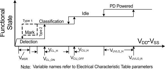 Figure 20. Threshold Voltages
8.4.1.2 PoE Start-Up Sequence
The waveforms of Figure 21 demonstrate detection, classification, and start-up from a PSE with type 2 hardware classification. The key waveforms shown are V(VDD-VSS), V(RTN-VSS), and IPI. IEEE 802.3at requires a minimum of two detection levels, two class and mark cycles, and start-up from the second mark event. VRTN to VSS falls as the TPS2379 charges CBULK following application of full voltage. In Figure 21, deassertion of the CDB signal is delayed and used to enable load current as seen in the IPI waveform.
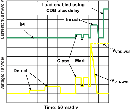 Figure 21. Start-up
8.4.1.3 Detection
The TPS2379 pulls DEN to VSS whenever V(VDD-VSS) is below the lower classification threshold. When the input voltage rises above VCL-ON, the DEN pin goes to an opendrain condition to conserve power. While in detection, RTN is high impedance, and almost all the internal circuits are disabled. An RDEN of 24.9 kΩ (±1%), presents the correct signature. It may be a small, low-power resistor because it only sees a stress of about 5 mW. A valid PD detection signature is an incremental resistance ( ΔV/ΔI ) between 23.75 kΩ and 26.25 kΩ at the PI.
The detection resistance seen by the PSE at the PI is the result of the input bridge resistance in series with the parallel combination of RDEN and internal VDD loading. The input diode bridge’s incremental resistance may be hundreds of ohms at the very low currents drawn when 2.7 V is applied to the PI. The input bridge resistance is partially compensated by the TPS2379's effective resistance during detection.
The type 2 hardware classification protocol of IEEE 802.3at specifies that a type 2 PSE drops its output voltage into the detection range during the classification sequence. The PD is required to have an incorrect detection signature in this condition, which is referred to as a mark event (see Figure 21). After the first mark event, the TPS2379 will present a signature less than 12 kΩ until it has experienced a V(VDD-VSS) voltage below the mark reset threshold (VMSR). This is explained more fully under Hardware Classification.
8.4.1.4 Hardware Classification
Hardware classification allows a PSE to determine a PD’s power requirements before powering, and helps with power management once power is applied. Type 2 hardware classification permits high power PSEs and PDs to determine whether the connected device can support high-power operation. A type 2 PD presents class 4 in hardware to indicate that it is a high-power device. A type 1 PSE will treat a class 4 device like a class 0 device, allotting 13 W if it chooses to power the PD. A PD that receives a 2-event class understands that it is powered from a high-power PSE and it may draw up to 25.5 W immediately after the 80 ms start-up period completes. A type 2 PD that does not receive a 2-event hardware classification may choose to not start, or must start in a 13 W condition and request more power through the DLL after start-up. The standard requires a type 2 PD to indicate that it is underpowered if this occurs. Start-up of a high-power PD under 13 W implicitly requires some form of powering down sections of the application circuits.
The maximum power entries in Table 1 determine the class the PD must advertise. The PSE may disconnect a PD if it draws more than its stated Class power, which may be the hardware class or a lower DLL-derived power level. The standard permits the PD to draw limited current peaks that increase the instantaneous power above the Table 1 limit, however the average power requirement always applies.
The TPS2379 implements two-event classification. Selecting an RCLS of 63.4 Ω provides a valid type 2 signature. TPS2379 may be used as a compatible type 1 device simply by programming class 0–3 per Table 1. DLL communication is implemented by the Ethernet communication system in the PD and is not implemented by the TPS2379.
The TPS2379 disables classification above VCU_OFF to avoid excessive power dissipation. CLS voltage is turned off during PD thermal limiting or when DEN is active. The CLS output is inherently current-limited, but should not be shorted to VSS for long periods of time.
Figure 22 shows how classification works for the TPS2379. Transition from state-to-state occurs when comparator thresholds are crossed (see Figure 19 and Figure 20). These comparators have hysteresis, which adds inherent memory to the machine. Operation begins at idle (unpowered by PSE) and proceeds with increasing voltage from left to right. A 2-event classification follows the (heavy lined) path towards the bottom, ending up with a latched type 2 decode along the lower branch that is highlighted. This state results in a low T2P during normal operation. Once the valid path to type 2 PSE detection is broken, the input voltage must transition below the mark reset threshold to start anew.
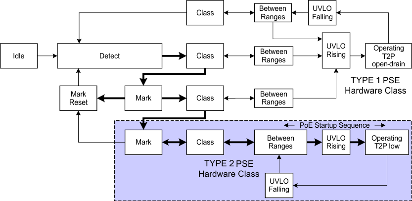 Figure 22. Two-Event Class Internal States
8.4.1.5 Inrush and Start-up
IEEE 802.3at has a start-up current and time limitation, providing type 2 PSE compatibility for type 1 PDs. A type 2 PSE limits output current to between 400 mA and 450 mA for up to 75 ms after power up (applying “48 V” to the PI) to mirror type 1 PSE functionality. The type 2 PSE will support higher output current after 75 ms. The TPS2379 implements a 140 mA inrush current, which is compatible with all PSE types. A high-power PD must limit its converter start-up peak current. The operational current cannot exceed 400 mA for a period of 80 ms or longer. This requirement implicitly requires some form of powering down sections of the application circuits.
8.4.1.6 Maintain Power Signature
The MPS is an electrical signature presented by the PD to assure the PSE that it is still present after operating voltage is applied. A valid MPS consists of a minimum DC current of 10 mA (or a 10 mA pulsed current for at least 75 ms every 325 ms) and an AC impedance lower than 26.3 kΩ in parallel with 0.05 μF. The AC impedance is usually accomplished by the minimum operating CBULK requirement of 5 μF. When DEN is used to force the hotswap switch off, the DC MPS will not be met. A PSE that monitors the DC MPS will remove power from the PD when this occurs. A PSE that monitors only the ac MPS may remove power from the PD.
8.4.1.7 Start-up and Operation
The internal PoE UVLO (Under Voltage Lock Out) circuit holds the hotswap switch off before the PSE provides full voltage to the PD. This prevents the downstream converter circuits from loading the PoE input during detection and classification. The converter circuits will discharge CBULK while the PD is unpowered. Thus V(VDD-RTN) will be a small voltage just after full voltage is applied to the PD, as seen in Figure 21. The PSE drives the PI voltage to the operating range once it has decided to power up the PD. When VVDD rises above the UVLO turnon threshold (VUVLO-R, approximately 38 V) with RTN high, the TPS2379 enables the hotswap MOSFET with an approximate 140 mA (inrush) current limit as seen in Figure 23. The CDB pin is active while CBULK charges and VRTN falls from VVDD to nearly VVSS. Once the inrush current falls about 10% below the inrush current limit, the PD current limit switches to the operational level (approximately 1000 mA) and CDB is deasserted to allow downstream converter circuitry to start. The TPS2379 asserts GATE after inrush is complete to enable an external pass MOSFET if used. In Figure 23, T2P is active because a type 2 PSE is plugged in.
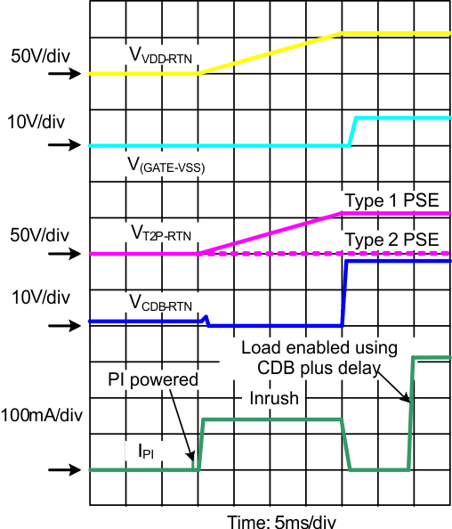 Figure 23. Power Up and Start
8.4.1.8 PD Hotswap Operation
IEEE 802.3at has taken a new approach to PSE output limiting. A type 2 PSE must meet an output current versus time template with specified minimum and maximum sourcing boundaries. The peak output current may be as high as 50 A for 10 μs or 1.75 A for 75 ms. This makes robust protection of the PD device even more important than it was in IEEE 802.3-2008.
The internal hotswap MOSFET is protected against output faults and input voltage steps with a current limit and deglitched (time-delay filtered) foldback. An overload on the pass MOSFET engages the current limit, with VRTN-VVSS rising as a result. GATE is pulled down about 300 μs after RTN current reaches the current limit level. If VRTN rises above approximately 12 V for longer than about 800 μs, the current limit reverts to the inrush value. The 800 μs deglitch feature prevents momentary transients from causing a PD reset, provided that recovery lies within the bounds of the hotswap and PSE protection. Figure 24 shows an example of the RTN current profile during VDD to RTN short circuit when only the internal hotswap MOSFET is used. The hotswap MOSFET goes into current limit, causing the RTN voltage to increase. Once VRTN exceeds 12V, IRTN which was clamped to the current limit drops to the level of inrush current limit after 800µs.
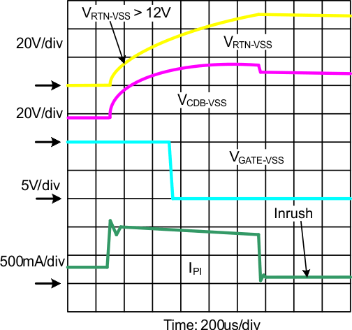 Figure 24. Response to PD Output Short Circuit Without AUX MOSFET
Figure 25 shows an example of the RTN current profile during VDD to RTN short circuit when the external MOSFET is used. The circuit is depicted in Figure 26. The current will divide between the internal and external MOSFETs. During the short circuit, the hotswap MOSFET goes into current limit, causing the RTN voltage to increase. When the internal MOSFET exceeds current limit for about 300 µs, GATE will deassert and shut off the auxiliary MOSFET. VRTN will rise quickly and the internal MOSFET will go into current limit for approximately 800 µs (after VRTN > about 12 V) and then IRTN which was clamped to the current limit drops into the inrush current limit.
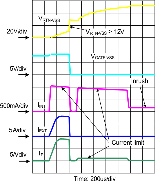 Figure 25. Response to PD Output Short Circuit With AUX MOSFET
The PD control has a thermal sensor that protects the internal hotswap MOSFET. Conditions like start-up or operation into a VDD -to-RTN short cause high power dissipation in the MOSFET. An over-temperature shutdown (OTSD) turns off the hotswap MOSFET and class regulator, which are restarted after the device cools. The hotswap MOSFET will be re-enabled with the inrush current limit when exiting from an over-temperature event. Pulling DEN to VSS during powered operation causes the internal hotswap MOSFET to turn off.
The hotswap switch will be forced off under the following conditions:
- V(DEN –VSS) < VPD_DIS when VVDD – VVSS is in the operational range,
- PD is over-temperature, or
- V(DEN – VSS) PoE UVLO falling threshold (about 32 V).
8.4.1.9 CDB and T2P
CDB (converter disable) is an active-low pin that indicates when the internal hotswap MOSFET is inrush limiting. CDB deasserts when inrush is over and can be used to enable a downstream converter to start up. Common interfaces to the converter controller include the soft start or enable pins.
T2P (type 2 PSE) is an active-low multifunction pin that indicates if (PSE = Type_2) and (PD current limit ≠ Inrush).
The usage of T2P is demonstrated in Figure 18. When PSE applies and PD observes a type 2 hardware classification, T2P pin is pulled to RTN as a indication of the type of PSE.
8.4.1.10 Auxiliary Pass MOSFET Control
The TPS2379 can be used in non-standard applications requiring power significantly above the IEEE802.3at, type 2 levels. This implementation can be achieved by utilizing all four Ethernet wire pairs and boosting the TPS2379 hotswap MOSFET operating current limit. Boosting the TPS2379 operating current limit is achieved by adding an external pass MOSFET to share the total load current with the internal hotswap MOSFET. The external pass MOSFET is enabled by the GATE pin after the internal hotswap MOSFET inrush is complete. The GATE pin will deassert if the TPS2379 internal current limit is exceeded in excess of 300 µs.
A comprehensive high power POE design example is discussed in application report Implementing a 60-W, End-to-End PoE System (SLVA498).