ZHCSBP7C October   2013  – December 2018 TPS24750 , TPS24751

UNLESS OTHERWISE NOTED, this document contains PRODUCTION DATA.  

  1. 特性
  2. 应用
  3. 说明
    1.     Device Images
      1.      应用原理图 (12V/10A)
      2.      瞬态输出短路响应
  4. 修订历史记录
  5. Device Comparison Table
  6. Pin Configuration and Functions
    1.     Pin Functions
  7. Specifications
    1. 7.1 Absolute Maximum Ratings
    2. 7.2 ESD Ratings
    3. 7.3 Recommended Operating Conditions
    4. 7.4 Thermal Information
    5. 7.5 Electrical Characteristics
    6. 7.6 Typical Characteristics
  8. Parameter Measurement Information
  9. Detailed Descriptions
    1. 9.1 Overview
    2. 9.2 Functional Block Diagram
    3. 9.3 Feature Description
      1. 9.3.1  DRAIN
      2. 9.3.2  EN
      3. 9.3.3  FLTb
      4. 9.3.4  GATE
      5. 9.3.5  GND
      6. 9.3.6  IMON
      7. 9.3.7  OUT
      8. 9.3.8  OV
      9. 9.3.9  PGb
      10. 9.3.10 PROG
      11. 9.3.11 SENSE
      12. 9.3.12 TIMER
      13. 9.3.13 VCC
    4. 9.4 Device Functional Modes
      1. 9.4.1 Board Plug-In
      2. 9.4.2 Inrush Operation
      3. 9.4.3 Action of the Constant-Power Engine
      4. 9.4.4 Circuit Breaker and Fast Trip
      5. 9.4.5 Automatic Restart
      6. 9.4.6 Start-Up with Short on Output
      7. 9.4.7 PGb, FLTb, and Timer Operations
        1. 9.4.7.1 Overtemperature Shutdown
        2. 9.4.7.2 Start-Up of Hot-Swap Circuit by VCC or EN
  10. 10Application and Implementation
    1. 10.1 Application Information
    2. 10.2 Typical Application
      1. 10.2.1 Design Requirements
      2. 10.2.2 Detailed Design Procedure
        1. 10.2.2.1 Power-Limited Start-Up
          1. 10.2.2.1.1 STEP 1. Choose RSENSE, RSET, and RIMON
          2. 10.2.2.1.2 STEP 2. Choose Power-Limit Value, PLIM, and RPROG
          3. 10.2.2.1.3 STEP 3. Choose Output Voltage Rising Time, tON, and Timing Capacitor CT
          4. 10.2.2.1.4 STEP 4. Calculate the Retry-Mode Duty Ratio
          5. 10.2.2.1.5 STEP 5. Select R1, R2, and R3 for UV and OV
          6. 10.2.2.1.6 STEP 6. Choose R4, R5, and C1
        2. 10.2.2.2 Alternative Design Example: Gate Capacitor (dv/dt) Control in Inrush Mode
        3. 10.2.2.3 Additional Design Considerations
          1. 10.2.2.3.1 Use of PGb
          2. 10.2.2.3.2 Output Clamp Diode
          3. 10.2.2.3.3 Gate Clamp Diode
          4. 10.2.2.3.4 Bypass Capacitors
          5. 10.2.2.3.5 Output Short-Circuit Measurements
      3. 10.2.3 Application Curves
    3. 10.3 System Examples
  11. 11Power Supply Recommendations
    1. 11.1 Transient Thermal Impedance
  12. 12Layout
    1. 12.1 Layout Guidelines
    2. 12.2 Layout Example
  13. 13器件和文档支持
    1. 13.1 文档支持
      1. 13.1.1 相关文档
    2. 13.2 相关链接
    3. 13.3 接收文档更新通知
    4. 13.4 社区资源
    5. 13.5 商标
    6. 13.6 静电放电警告
    7. 13.7 Export Control Notice
    8. 13.8 术语表
  14. 14机械、封装和可订购信息

封装选项

机械数据 (封装 | 引脚)
散热焊盘机械数据 (封装 | 引脚)
订购信息

Typical Characteristics

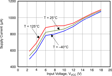
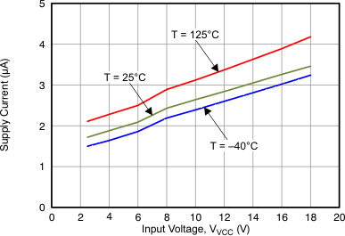
TPS24750 TPS24751 Figure_06_LVSAL1.gif
EN = High
Figure 1. Supply Current vs Input Voltage at Normal Operation
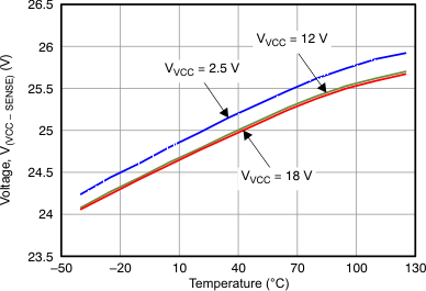
TPS24750 TPS24751 Figure_08_LVSAL1.gif
Figure 3. Voltage Across RSENSE in Inrush Current Limiting vs Temperature
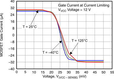
TPS24750 TPS24751 Figure_10_LVSAL1.gif
Figure 5. Internal FET Gate Current vs Voltage Across RSENSE During Inrush Power Limiting
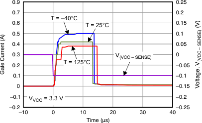
TPS24750 TPS24751 Figure_12_LVSAL1.gif
VVCC = VGATE = 3.3 V
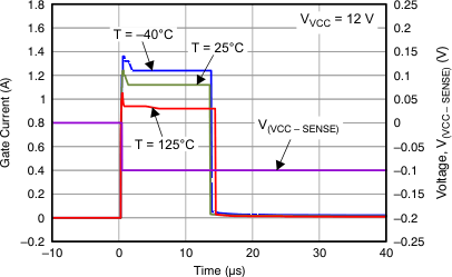
Figure 7. Gate Current During Fast Trip
TPS24750 TPS24751 Figure_14_LVSAL1.gif
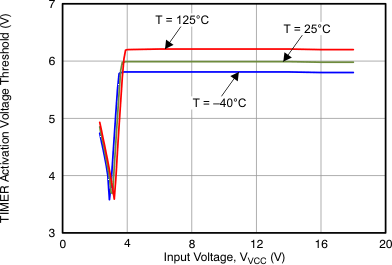
Figure 9. TIMER Activation Voltage Threshold vs Input Voltage at Various Temperatures
TPS24750 TPS24751 Figure_04_slvsc87.gif
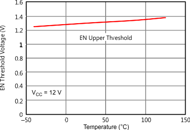
Figure 11. EN Threshold Voltage vs Temperature
TPS24750 TPS24751 Figure_18_LVSAL1.gif
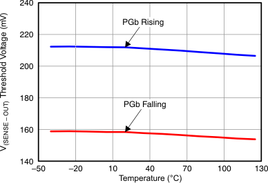
Figure 13. Threshold Voltage of VDS vs Temperature, PGb Rising and Falling
TPS24750 TPS24751 Figure_20_LVSAL1.gif
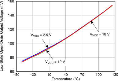
Figure 15. PGb Open-Drain Output Voltage in Low State
TPS24750 TPS24751 Figure_23_LVSAL1.gif
Figure 17. Supply Current vs Input Voltage at Various Temperatures when EN Pulled Low
TPS24750 TPS24751 Figure_25_LVSAL1.gif
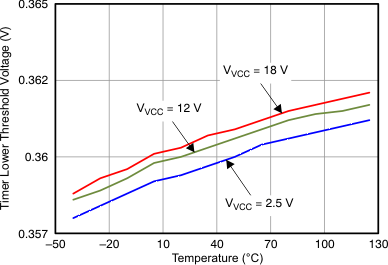
Figure 19. Timer Lower Threshold Voltage vs Temperature at Various Input Voltages
TPS24750 TPS24751 Figure_27_LVSAL1.gif
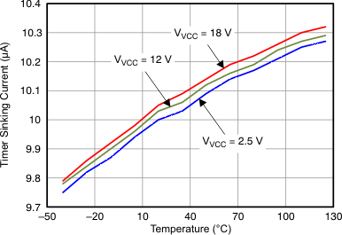
Figure 21. Timer Sinking Current vs Temperature at Various Input Voltages
TPS24750 TPS24751 Figure_01_LVSC87.gif
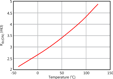
Figure 23. RDS(ON) vs Temperature
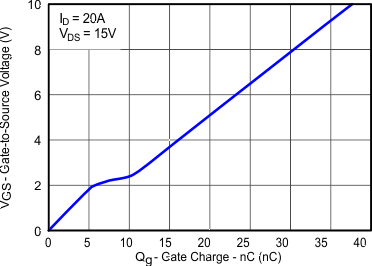
TPS24750 TPS24751 gate_charge_graph_LVSC87.gif
Figure 25. Gate Charge – Internal MOSFET
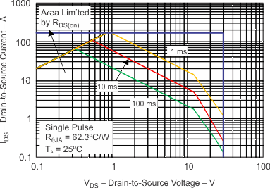
TPS24750 TPS24751 G010_slvsc87.gif
Figure 27. TPS2475x Maximum Safe Operating Area (SOA)
TPS24750 TPS24751 Figure_07_LVSAL1.gif
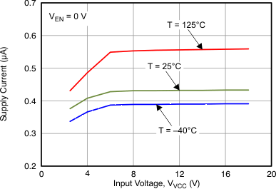
EN = 0 V
Figure 2. Supply Current vs Input Voltage at Shutdown
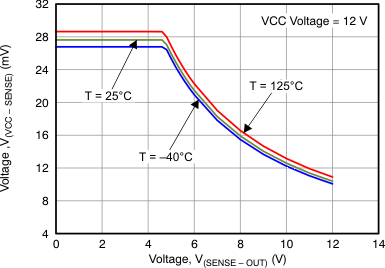
TPS24750 TPS24751 Figure_09_LVSAL1.gif
Figure 4. Voltage Across RSENSE in Inrush Power Limiting vs VDS of Internal FET
TPS24750 TPS24751 Figure_11_LVSAL1.gif
VVCC = VGATE = 12 V
Figure 6. Gate Current During Fast Trip
TPS24750 TPS24751 Figure_13_LVSAL1.gif
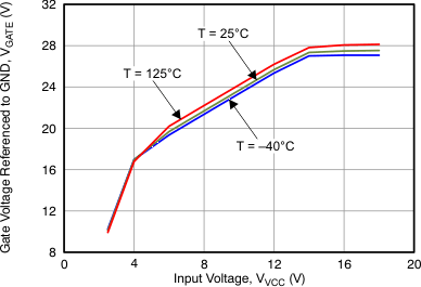
Figure 8. Gate Voltage With Zero Gate Current vs Input Voltage
TPS24750 TPS24751 Figure_15_LVSAL1.gif
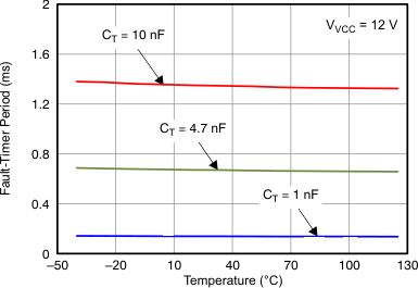
Figure 10. Fault-Timer vs Temperature with Various TIMER Capacitors
TPS24750 TPS24751 Figure_17_LVSAL1.gif
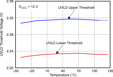
Figure 12. UVLO Threshold Voltage vs Temperature
TPS24750 TPS24751 Figure_19_LVSAL1.gif
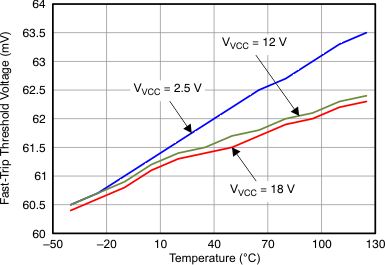
Figure 14. Fast-Trip Threshold Voltage vs Temperature
TPS24750 TPS24751 Figure_21_LVSAL1.gif
Figure 16. FLTb Open-Drain Output Voltage in Low State
TPS24750 TPS24751 Figure_24_LVSAL1.gif
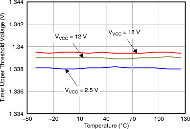
Figure 18. Timer Upper Threshold Voltage vs Temperature at Various Input Voltages
TPS24750 TPS24751 Figure_26_LVSAL1.gif
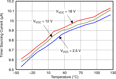
Figure 20. Timer Sourcing Current vs Temperature at Various Input Voltages
TPS24750 TPS24751 Figure_05_slvsc87.gif
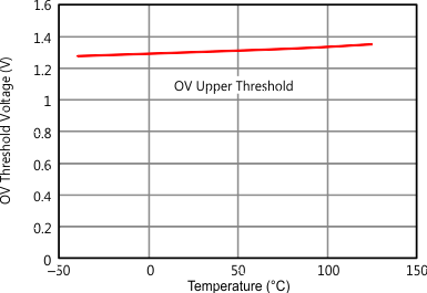
Figure 22. OV Threshold Voltage vs Temperature
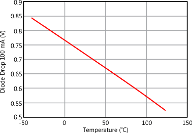
TPS24750 TPS24751 Figure_02_LVSC87.gif
Figure 24. Diode Drop vs Temperature
TPS24750 TPS24751 Figure_03_LVSC87.gif
Figure 26. Leakage Current vs Temperature