ZHCSBP7C October 2013 – December 2018 TPS24750 , TPS24751
UNLESS OTHERWISE NOTED, this document contains PRODUCTION DATA.
- 1 特性
- 2 应用
- 3 说明
- 4 修订历史记录
- 5 Device Comparison Table
- 6 Pin Configuration and Functions
- 7 Specifications
- 8 Parameter Measurement Information
-
9 Detailed Descriptions
- 9.1 Overview
- 9.2 Functional Block Diagram
- 9.3 Feature Description
- 9.4 Device Functional Modes
-
10Application and Implementation
- 10.1 Application Information
- 10.2
Typical Application
- 10.2.1 Design Requirements
- 10.2.2
Detailed Design Procedure
- 10.2.2.1
Power-Limited Start-Up
- 10.2.2.1.1 STEP 1. Choose RSENSE, RSET, and RIMON
- 10.2.2.1.2 STEP 2. Choose Power-Limit Value, PLIM, and RPROG
- 10.2.2.1.3 STEP 3. Choose Output Voltage Rising Time, tON, and Timing Capacitor CT
- 10.2.2.1.4 STEP 4. Calculate the Retry-Mode Duty Ratio
- 10.2.2.1.5 STEP 5. Select R1, R2, and R3 for UV and OV
- 10.2.2.1.6 STEP 6. Choose R4, R5, and C1
- 10.2.2.2 Alternative Design Example: Gate Capacitor (dv/dt) Control in Inrush Mode
- 10.2.2.3 Additional Design Considerations
- 10.2.2.1
Power-Limited Start-Up
- 10.2.3 Application Curves
- 10.3 System Examples
- 11Power Supply Recommendations
- 12Layout
- 13器件和文档支持
- 14机械、封装和可订购信息
9.4.5 Automatic Restart
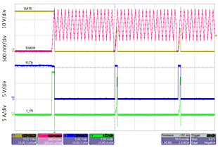
In Auto-retry versions (TPS24751), device automatically initiates a restart after a fault has caused it to turnoff the internal FET. Internal control circuits use CT to count 16 cycles before re-enabling the FET as shown in Figure 37. This sequence repeats if the fault persists. The timer has a 1:1 charge-to-discharge current ratio. For the very first cycle, the TIMER pin starts from 0 V and rises to the upper threshold of 1.35 V and subsequently falls to 0.35 V before restarting. For the following 16 cycles, 0.35 V is used as the lower threshold. This small duty cycle often reduces the average short-circuit power dissipation to levels associated with normal operation and eliminates special thermal considerations for surviving a prolonged output short.
 Figure 37. Auto-Restart Cycle Timing
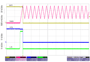
  Figure 38. Latch After Overload Fault