ZHCSBP7C October 2013 – December 2018 TPS24750 , TPS24751
UNLESS OTHERWISE NOTED, this document contains PRODUCTION DATA.
- 1 特性
- 2 应用
- 3 说明
- 4 修订历史记录
- 5 Device Comparison Table
- 6 Pin Configuration and Functions
- 7 Specifications
- 8 Parameter Measurement Information
-
9 Detailed Descriptions
- 9.1 Overview
- 9.2 Functional Block Diagram
- 9.3 Feature Description
- 9.4 Device Functional Modes
-
10Application and Implementation
- 10.1 Application Information
- 10.2
Typical Application
- 10.2.1 Design Requirements
- 10.2.2
Detailed Design Procedure
- 10.2.2.1
Power-Limited Start-Up
- 10.2.2.1.1 STEP 1. Choose RSENSE, RSET, and RIMON
- 10.2.2.1.2 STEP 2. Choose Power-Limit Value, PLIM, and RPROG
- 10.2.2.1.3 STEP 3. Choose Output Voltage Rising Time, tON, and Timing Capacitor CT
- 10.2.2.1.4 STEP 4. Calculate the Retry-Mode Duty Ratio
- 10.2.2.1.5 STEP 5. Select R1, R2, and R3 for UV and OV
- 10.2.2.1.6 STEP 6. Choose R4, R5, and C1
- 10.2.2.2 Alternative Design Example: Gate Capacitor (dv/dt) Control in Inrush Mode
- 10.2.2.3 Additional Design Considerations
- 10.2.2.1
Power-Limited Start-Up
- 10.2.3 Application Curves
- 10.3 System Examples
- 11Power Supply Recommendations
- 12Layout
- 13器件和文档支持
- 14机械、封装和可订购信息
10.3 System Examples
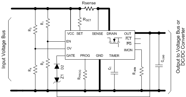
 Figure 47. Negative Voltage Gate Protection
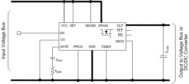
 The TPS2475x can be configured as a high current load switch with low external part count. The schematic diagram of load switch configuration is shown in Figure 48. The output voltage ramp rate is controlled with RC circuit (Rgate and Cgate) at the Gate pin of the device. For detailed design process refer to the application note 12-A Integrated Load Switch Using TPS24750/51.
Due to their robust protection features along with low RDS(on) of 3 mΩ integrated MOSFET and precise current-limiting, the TPS2475x eFuses finds usage in power supply modules for Position Encoder Interfaces in applications such as Servo Drives and Position Control. Refer to the following TI Designs for system usage examples of the TPS2475x in these applications.
Power Supply with Programmable Output Voltage and Protection for Position Encoder Interfaces
Interface to a 5-V BiSS® Position Encoder
 Figure 48. TPS2475x Configured as Simple 12-A Load Switch