ZHCSAX0C February 2013 – July 2016 TPS2546
PRODUCTION DATA.
- 1 特性
- 2 应用
- 3 说明
- 4 修订历史记录
- 5 Pin Configuration and Functions
- 6 Specifications
- 7 Parameter Measurement Information
-
8 Detailed Description
- 8.1 Overview
- 8.2 Functional Block Diagram
- 8.3
Feature Description
- 8.3.1 Standard Downstream Port (SDP) USB 2.0/USB 3.0
- 8.3.2 Charging Downstream Port (CDP)
- 8.3.3 Dedicated Charging Port (DCP)
- 8.3.4 Wake on USB Feature (Mouse/Keyboard Wake Feature)
- 8.3.5 Load Detect
- 8.3.6 Power Wake
- 8.3.7 Port Power Management (PPM)
- 8.3.8 Overcurrent Protection
- 8.3.9 FAULT Response
- 8.3.10 Undervoltage Lockout (UVLO)
- 8.3.11 Thermal Sense
- 8.4 Device Functional Modes
- 9 Application and Implementation
- 10Power Supply Recommendations
- 11Layout
- 12器件和文档支持
- 13机械、封装和可订购信息
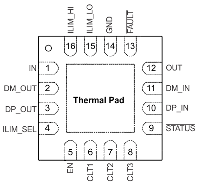
5 Pin Configuration and Functions
RTE Package
16-Pin WQFN
Top View

Pin Functions
| PIN | TYPE(1) | DESCRIPTION | |
|---|---|---|---|
| NO. | NAME | ||
| 1 | IN | P | Input voltage and supply voltage; connect 0.1 μF or greater ceramic capacitor from IN to GND as close to the device as possible. |
| 2 | DM_OUT | I/O | D– data line to USB host controller. |
| 3 | DP_OUT | I/O | D+ data line to USB host controller. |
| 4 | ILIM_SEL | I | Logic-level input signal used to control the charging mode, current limit threshold, and load detection; see Table 3. Can be tied directly to IN or GND without pullup or pulldown resistor. |
| 5 | EN | I | Logic-level input for turning the power switch and the signal switches on/off; logic low turns off the signal and power switches and holds OUT in discharge. Can be tied directly to IN or GND without pullup or pulldown resistor. |
| 6 | CTL1 | I | Logic-level inputs used to control the charging mode and the signal switches; see Table 3. Can be tied directly to IN or GND without pullup or pulldown resistor. |
| 7 | CTL2 | I | |
| 8 | CTL3 | I | |
| 9 | STATUS | O | Active-low open-drain output, asserted in load detection conditions. |
| 10 | DP_IN | I/O | D+ data line to downstream connector. |
| 11 | DM_IN | I/O | D– data line to downstream connector. |
| 12 | OUT | P | Power-switch output. |
| 13 | FAULT | O | Active-low open-drain output, asserted during overtemperature or current limit conditions. |
| 14 | GND | P | Ground connection. |
| 15 | ILIM_LO | I | External resistor connection used to set the low current-limit threshold and the load detection current threshold. A resistor to ILIM_LO is optional; see Current-Limit Settings in Detailed Description. |
| 16 | ILIM_HI | I | External resistor connection used to set the high-current-limit threshold. |
| — | Thermal Pad | — | Internally connected to GND; used to heatsink the part to the circuit board traces. Connect to GND plane. |
(1) G = ground, I = input, O = output, P = power.