SLVS363G August 2001 – September 2016 TPS3103 , TPS3106 , TPS3110
PRODUCTION DATA.
- 1 Features
- 2 Applications
- 3 Description
- 4 Revision History
- 5 Available Options
- 6 Pin Configuration and Functions
- 7 Specifications
- 8 Detailed Description
- 9 Application and Implementation
- 10Power Supply Recommendations
- 11Layout
- 12Device and Documentation Support
- 13Mechanical, Packaging, and Orderable Information
9 Application and Implementation
NOTE
Information in the following applications sections is not part of the TI component specification, and TI does not warrant its accuracy or completeness. TI’s customers are responsible for determining suitability of components for their purposes. Customers should validate and test their design implementation to confirm system functionality.
9.1 Application Information
The TPS310x and TPS311x families are supervisory circuits made to monitor the input supply and other external voltages greater than 0.551 V. These devices are made to operate from and monitor input supplies ranging from 0.9 V to 3.6 V, and all versions have a manual reset pin. The TPS3103 and TPS3106 both have an active-low, open-drain RESET output. The TPS3103 device has an integrated power-fail input (PFI) and corresponding power-fail output (PFO) that can be used for low-battery detection or for monitoring a power supply other than the input supply and has a short delay time for more immediate triggering of the output. The TPS3106 device has a SENSE input with a corresponding output (RSTSENSE) for monitoring voltages other than the input supply and a longer delay time than the TPS3103 device to minimize accidental triggering of the output. The TPS3110 device has an active-low push/pull RESET and a watchdog timer that is used for monitoring the operation of microprocessors.
9.2 Typical Application
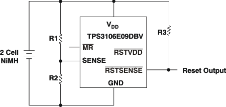
 Figure 17. Battery Monitoring With 3-μA Supply Current for Device and Resistor Divider
9.2.1 Design Requirements
In some applications it is necessary to minimize the quiescent current even during the reset period. This is especially true when the voltage of a battery is supervised and the RESET is used to shut down the system or for an early warning. In this case the reset condition will last for a longer period of time. The current drawn from the battery should almost be zero, especially when the battery is discharged.
For this kind of application, either the TPS3103 or TPS3106 device is a good fit. To minimize current consumption, select a version where the threshold voltage is lower than the voltage monitored at VDD. The TPS3106 device has two reset outputs. One output (RSTVDD) is triggered from the voltage monitored at VDD. The other output (RSTSENSE) is triggered from the voltage monitored at SENSE. In the application shown in Figure 17, the TPS3106E09 device is used to monitor the input voltage of two NiCd or NiMH cells. The threshold voltage [V(TH) = 0.86 V] was chosen as low as possible to ensure that the supply voltage is always higher than the threshold voltage at VDD. The voltage of the battery is monitored using the SENSE input.
9.2.2 Detailed Design Procedure
The voltage divider was calculated to assert a reset using the RSTSENSE output at 2 × 0.8 V = 1.6 V, using Equation 1.

where
- VTRIP is the voltage of the battery at which a reset is asserted
- VIT–(S) is the threshold voltage at SENSE = 0.551 V
- R1 was chosen for a resistor current in the 1-μA range
- With VTRIP = 1.6 V
- R1 ≡ 1.9 × R2
- R1 = 820 kΩ, R2 = 430 kΩ
