SLVS363G August 2001 – September 2016 TPS3103 , TPS3106 , TPS3110
PRODUCTION DATA.
- 1 Features
- 2 Applications
- 3 Description
- 4 Revision History
- 5 Available Options
- 6 Pin Configuration and Functions
- 7 Specifications
- 8 Detailed Description
- 9 Application and Implementation
- 10Power Supply Recommendations
- 11Layout
- 12Device and Documentation Support
- 13Mechanical, Packaging, and Orderable Information
8 Detailed Description
8.1 Overview
The TPS310x and TPS311x families of supervisory circuits operate from supply voltages from 0.9 V to 3.6 V and provide circuit initialization and timing supervision for DSP- and processor-based systems. During power-on, RESET is asserted when the supply voltage (VDD) exceeds 0.4 V. The devices monitor VDD and keep the RESET output low as long as VDD remains below the threshold voltage (VIT–). To ensure proper system reset, after VDD surpasses the threshold voltage plus the hysteresis (VIT– + VHYS) an internal timer delays the transition of the RESET signal from low to high for the specified time. The delay time starts after VDD has risen above (VIT– + VHYS). When VDD drops below VIT–, the output becomes active again.
All the devices of this family have a fixed-VDD threshold voltage (VIT–) set by an internal voltage divider. The TPS3103 and TPS3106 devices both have an active-low, open-drain RESET output. The TPS3103 device has an integrated power-fail input (PFI) and corresponding power-fail output (PFO) that can be used for low-battery detection or for monitoring a power supply other than the input supply. The TPS3106 device has a SENSE input with a corresponding output (RSTSENSE) for monitoring voltages other than the input supply. The TPS3110 device has an active-low push/pull RESET and a watchdog timer that is used for monitoring the operation of microprocessors. All three devices have manual reset pin (MR) that can be used to force the outputs low regardless of the sensed voltages.
8.2 Functional Block Diagrams
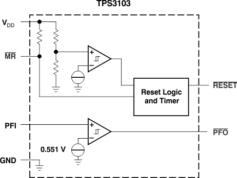 Figure 12. TPS3103 Functional Block Diagram
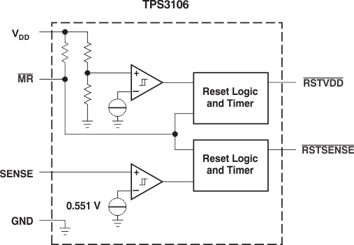 Figure 13. TPS3106 Functional Block Diagram
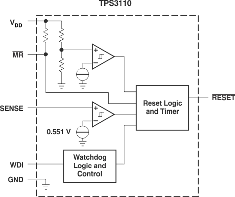 Figure 14. TPS3110 Functional Block Diagram
8.3 Feature Description
8.3.1 Watchdog
The TPS3110 device integrates a watchdog timer that must be periodically triggered by a positive or negative transition of WDI. When the supervising system fails to retrigger the watchdog circuit within the time-out interval, RESET becomes active for the time period (tD). This event also reinitializes the watchdog timer.
8.3.2 Manual Reset (MR)
Many μC-based products require manual-reset capability, allowing an operator or logic circuitry to initiate a reset. Logic low at MR asserts reset. Reset remains asserted while MR is low and for a time period (tD) after MR returns high. The input has an internal 100-kΩ pullup resistor, so it can be left open if it is unused.
Connect a normally open momentary switch from MR to GND to create a manual reset function. External debounce is not required. If MR is driven from long cables or if the device is used in noisy environments, connecting a 0.1-μF capacitor from MR to GND provides additional noise immunity.
If there is a possibility of transient or DC conditions causing MR to rise above VDD, a diode should be used to limit MR to a diode drop above VDD.
8.3.3 PFI, PFO
The TPS3103 has an integrated power-fail (PFI) comparator with a separate open-drain (PFO) output. The PFI and PFO can be used for low-battery detection, power-fail warning, or for monitoring a power supply other than the main supply, and has no effect on RESET.
An additional comparator is provided to monitor voltages other than the nominal supply voltage. The power-fail input (PFI) will be compared with an internal voltage reference of 0.551 V. If the input voltage falls below the power-fail threshold (VIT – (S)), the power-fail output (PFO) goes low. If it goes above 0.551 V plus approximately 15-mV hysteresis, the output returns to high. By connecting two external resistors, it is possible to supervise any voltage above 0.551 V. The sum of both resistors should be approximately 1 MΩ, to minimize power consumption and to assure that the current into the PFI pin can be neglected, compared with the current through the resistor network. The tolerance of the external resistors should be not more than 1% to ensure minimal variation of sensed voltage. If the power-fail comparator is unused, connect PFI to GND and leave PFO unconnected. For proper operation of the PFI-comparator, the supply voltage (VDD) must be higher than 0.8 V.
8.3.4 SENSE
The voltage at the SENSE input is compared with a reference voltage of 0.551 V. If the voltage at SENSE falls below the sense-threshold (VIT − (S)), reset is asserted. On the TPS3106 device, a dedicated RSTSENSE output is available. On the TPS3110 device, the logic signal from SENSE is OR-wired with the logic signal from VDD or MR. An internal timer delays the return of the output to the inactive state, once the voltage at SENSE goes above 0.551 V plus about 15 mV of hysteresis. For proper operation of the SENSE-comparator, the supply voltage must be higher than 0.8 V.
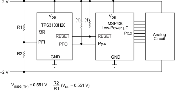
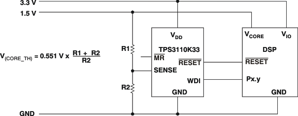 Figure 16. TPS3110 in a DSP-System Monitoring Both Supply Voltages
8.4 Device Functional Modes
Table 1. TPS3103 Function Table
| MR | V(PFI) > 0.551 V | VDD > VIT– | RESET | PFO |
|---|---|---|---|---|
| L | 0 | X(1) | L | L |
| L | 1 | X | L | H |
| H | 0 | 0 | L | L |
| H | 0 | 1 | H | L |
| H | 1 | 0 | L | H |
| H | 1 | 1 | H | H |
Table 2. TPS3106 Function Table
| MR | V(SENSE) > 0.551 V | VDD > VIT– | RSTVDD | RSTSENSE |
|---|---|---|---|---|
| L | X(1) | X | L | L |
| H | 0 | 0 | L | L |
| H | 0 | 1 | H | L |
| H | 1 | 0 | L | H |
| H | 1 | 1 | H | H |