SLVS363G August   2001  – September 2016 TPS3103 , TPS3106 , TPS3110

PRODUCTION DATA.  

  1. Features
  2. Applications
  3. Description
  4. Revision History
  5. Available Options
  6. Pin Configuration and Functions
  7. Specifications
    1. 7.1 Absolute Maximum Ratings
    2. 7.2 ESD Ratings
    3. 7.3 Recommended Operating Conditions
    4. 7.4 Thermal Information
    5. 7.5 Electrical Characteristics
    6. 7.6 Timing Requirements
    7. 7.7 Switching Characteristics
    8. 7.8 Typical Characteristics
  8. Detailed Description
    1. 8.1 Overview
    2. 8.2 Functional Block Diagrams
    3. 8.3 Feature Description
      1. 8.3.1 Watchdog
      2. 8.3.2 Manual Reset (MR)
      3. 8.3.3 PFI, PFO
      4. 8.3.4 SENSE
    4. 8.4 Device Functional Modes
  9. Application and Implementation
    1. 9.1 Application Information
    2. 9.2 Typical Application
      1. 9.2.1 Design Requirements
      2. 9.2.2 Detailed Design Procedure
      3. 9.2.3 Application Curve
  10. 10Power Supply Recommendations
  11. 11Layout
    1. 11.1 Layout Guidelines
    2. 11.2 Layout Example
  12. 12Device and Documentation Support
    1. 12.1 Device Support
      1. 12.1.1 Development Support
        1. 12.1.1.1 Spice Models
      2. 12.1.2 Device Nomenclature
    2. 12.2 Related Links
    3. 12.3 Receiving Notification of Documentation Updates
    4. 12.4 Community Resources
    5. 12.5 Trademarks
    6. 12.6 Electrostatic Discharge Caution
    7. 12.7 Glossary
  13. 13Mechanical, Packaging, and Orderable Information

封装选项

请参考 PDF 数据表获取器件具体的封装图。

机械数据 (封装 | 引脚)
  • DBV|6
散热焊盘机械数据 (封装 | 引脚)
订购信息

11 Layout

11.1 Layout Guidelines

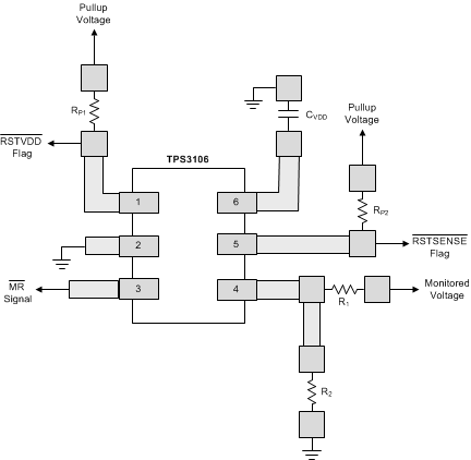
Follow these guidelines to lay out the printed-circuit-board (PCB) that is used for the TPS310x and TPS3110x family of devices.

  • Place the VDD decoupling capacitor close to the device.
  • Avoid using long traces for the VCC supply node. The VCC capacitor (CVDD), along with parasitic inductance from the supply to the capacitor, can form an LC tank and create ringing with peak voltages above the maximum VDD voltage.

11.2 Layout Example
TPS3103 TPS3106 TPS3110 layout_dbv_lvs363.gif Figure 19. Example Layout (DBV Package)