ZHCS155C March 2011 – November 2023 TPS40170
PRODUCTION DATA
- 1
- 1 特性
- 2 应用
- 3 说明
- 4 Pin Configuration and Functions
- 5 Specifications
-
6 Detailed Description
- 6.1 Overview
- 6.2 Functional Block Diagram
- 6.3
Feature Description
- 6.3.1 LDO Linear Regulators and Enable
- 6.3.2 Input Undervoltage Lockout (UVLO)
- 6.3.3 Oscillator and Voltage Feed-Forward
- 6.3.4 Overcurrent Protection and Short-Circuit Protection (OCP and SCP)
- 6.3.5 Soft-Start and Fault-Logic
- 6.3.6 Overtemperature Fault
- 6.3.7 Tracking
- 6.3.8 Adaptive Drivers
- 6.3.9 Start-Up into Pre-Biased Output
- 6.3.10 Power Good (PGOOD)
- 6.3.11 PGND and AGND
- 6.4 Device Functional Modes
-
7 Application and Implementation
- 7.1 Application Information
- 7.2
Typical Application
- 7.2.1 Design Requirements
- 7.2.2
Detailed Design Procedure
- 7.2.2.1 Custom Design with WEBENCH® Tools
- 7.2.2.2 List of Materials
- 7.2.2.3 Select a Switching Frequency
- 7.2.2.4 Inductor Selection (L1)
- 7.2.2.5 Output Capacitor Selection (C9)
- 7.2.2.6 Peak Current Rating of Inductor
- 7.2.2.7 Input Capacitor Selection (C1, C6)
- 7.2.2.8 MOSFET Switch Selection (Q1, Q2)
- 7.2.2.9 Timing Resistor (R7)
- 7.2.2.10 UVLO Programming Resistors (R2, R6)
- 7.2.2.11 Boot-Strap Capacitor (C7)
- 7.2.2.12 VIN Bypass Capacitor (C18)
- 7.2.2.13 VBP Bypass Capacitor (C19)
- 7.2.2.14 VDD Bypass Capacitor (C16)
- 7.2.2.15 SS Timing Capacitor (C15)
- 7.2.2.16 ILIM Resistor (R9, C17)
- 7.2.2.17 SCP Multiplier Selection (R5)
- 7.2.2.18 Feedback Divider (R10, R11)
- 7.2.2.19 Compensation: (R4, R13, C13, C14, C21)
- 7.2.3 Application Curves
- 7.3 Power Supply Recommendations
- 7.4 Layout
- 8 Device and Documentation Support
- 9 Revision History
- 10Mechanical, Packaging, and Orderable Information
6.4.1 Frequency Synchronization
The TPS40170 has three modes.
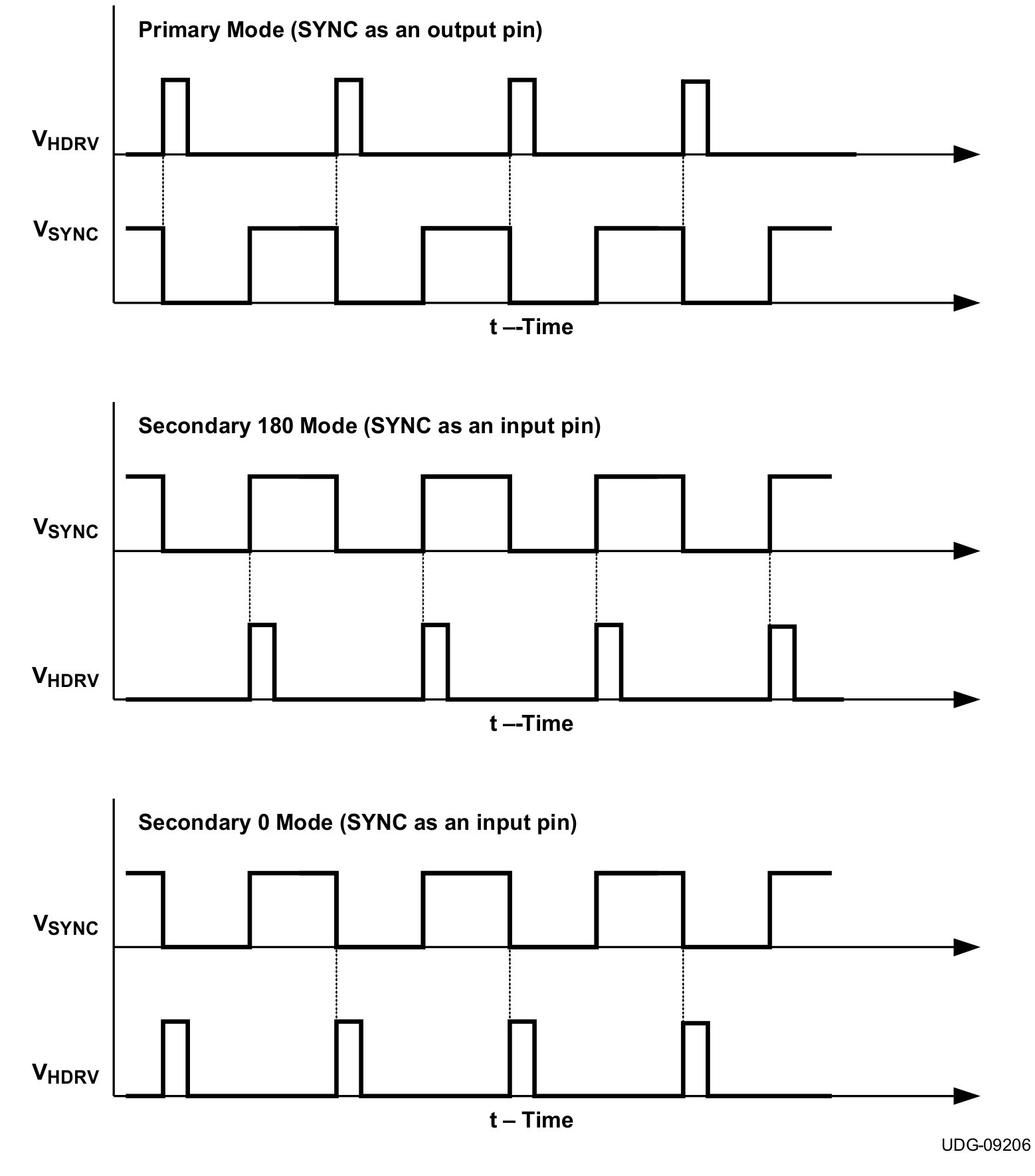
- Primary mode: In this mode the primary/secondary selector pin, (M/S) is connected to VIN. The SYNC pin emits a stream of pulses at the same frequency as the PWM switching frequency. The pulse stream at the SYNC pin is at 50% duty cycle and the same amplitude as VVBP. Also, the falling edge of the voltage on SYNC pin is synchronized with the rising edge of the HDRV.
- Secondary-180° mode: In this mode the M/S pin is connected to GND. The SYNC pin of the TPS40170 accepts a synchronization clock signal, and the HDRV is synchronized with the rising edge of the incoming synchronization clock.
- Secondary-0° mode: In this mode, the M/S pin is left open. The SYNC pin of the TPS40170 accepts a synchronization clock signal, and the HDRV is synchronized with the falling edge of the incoming synchronization clock.
The two secondary modes can be synchronized to an external clock through the SYNC pin. They are shown in Figure 6-18. The synchronization frequency must be within ±30% of its programmed free running frequency.
 Figure 6-18 Frequency Synchronization Waveforms In
Different Modes
Figure 6-18 Frequency Synchronization Waveforms In
Different ModesTPS40170 provides a smooth transition for the SYNC clock signal loss at secondary mode. In secondary mode, a synchronization clock signal is provided externally through the SYNC pin to the device. The switching frequency is synchronized to the external SYNC clock signal. If for some reason the external clock signal is missing, the device switching frequency is automatically overridden by a transition frequency which is 0.7 times its programmed free running frequency. This transition time is approximately 20 μs. After that, the device switching frequency is changed to its programmed free running frequency. Figure 6-19 shows this process.
 Figure 6-19 Transition for Sync Clock Signal
Missing (For Secondary-180 Mode)
 When the device is operating in the primary mode with duty ratio around 50%, PWM jittering can occur. Always configure the device into the secondary mode by either connecting the M/S pin to GND or leaving it floating if primary mode is not used.
When an external SYNC clock signal is used for synchronization, limit maximum slew rate of the clock signal to 10 V/µs to avoid potential PWM jittering and connect the SYNC pin to the external clock signal via a 5-kΩ resistor.