ZHCSI35C November   2009  – April 2018 TPS51200-Q1

PRODUCTION DATA.  

  1. 特性
  2. 应用
  3. 说明
    1.     Device Images
      1.      标准 DDR 应用
  4. 修订历史记录
  5. Pin Configuration and Functions
    1.     Pin Functions
  6. Specifications
    1. 6.1 Absolute Maximum Ratings
    2. 6.2 ESD Ratings
    3. 6.3 Recommended Operating Conditions
    4. 6.4 Thermal Information
    5. 6.5 Electrical Characteristics
    6. 6.6 Switching Characteristics
    7. 6.7 Typical Characteristics
  7. Detailed Description
    1. 7.1 Overview
    2. 7.2 Functional Block Diagram
    3. 7.3 Feature Description
      1. 7.3.1 Sink and Source Regulator (VO Pin)
      2. 7.3.2 Reference Input (REFIN Pin)
      3. 7.3.3 Reference Output (REFOUT Pin)
      4. 7.3.4 Soft-Start Sequencing
      5. 7.3.5 Enable Control (EN Pin)
      6. 7.3.6 Powergood Function (PGOOD Pin)
      7. 7.3.7 Current Protection (VO Pin)
      8. 7.3.8 UVLO Protection (VIN Pin)
      9. 7.3.9 Thermal Shutdown
    4. 7.4 Device Functional Modes
      1. 7.4.1 S3 and Pseudo-S5 Support
      2. 7.4.2 Tracking Startup and Shutdown
  8. Application and Implementation
    1. 8.1 Application Information
    2. 8.2 Typical Application
      1. 8.2.1 VTT DIMM Applications
        1. 8.2.1.1 Design Parameters
        2. 8.2.1.2 Detailed Design Procedure
          1. 8.2.1.2.1 VIN Capacitor
          2. 8.2.1.2.2 VLDO Input Capacitor
          3. 8.2.1.2.3 Output Capacitor
          4. 8.2.1.2.4 Output Tolerance Consideration for VTT DIMM Applications
        3. 8.2.1.3 Application Curves
      2. 8.2.2 Design Example 1
        1. 8.2.2.1 Design Parameters
      3. 8.2.3 Design Example 2
        1. 8.2.3.1 Design Parameters
      4. 8.2.4 Design Example 3
        1. 8.2.4.1 Design Parameters
      5. 8.2.5 Design Example 4
        1. 8.2.5.1 Design Parameters
      6. 8.2.6 Design Example 5
        1. 8.2.6.1 Design Parameters
      7. 8.2.7 Design Example 6
        1. 8.2.7.1 Design Parameters
      8. 8.2.8 Design Example 7
        1. 8.2.8.1 Design Parameters
  9. Power Supply Recommendations
  10. 10Layout
    1. 10.1 Layout Guidelines
    2. 10.2 Layout Example
    3. 10.3 Thermal Considerations
  11. 11器件和文档支持
    1. 11.1 器件支持
      1. 11.1.1 Third-Party Products Disclaimer
    2. 11.2 文档支持
      1. 11.2.1 相关文档
    3. 11.3 接收文档更新通知
    4. 11.4 社区资源
    5. 11.5 商标
    6. 11.6 静电放电警告
    7. 11.7 Glossary
  12. 12机械、封装和可订购信息

封装选项

机械数据 (封装 | 引脚)
散热焊盘机械数据 (封装 | 引脚)
订购信息

Tracking Startup and Shutdown

The TPS51200-Q1 device also supports tracking startup and shutdown when the EN pin is tied directly to the system bus and not used to turn on or turn off the device. During tracking startup, the VO pin follows the REFOUT pin when the REFIN voltage is greater than 0.39 V. The REFIN pin follows the rise of the VDDQ rail though a voltage divider. The typical soft-start time for the VDDQ rail is approximately 3 ms, however this soft-star time can vary depending on the system configuration. The SS time of the VO output no longer depends on the OCL setting, but is a function of the SS time of the VDDQ rail. PGOOD is asserted 2 ms after the VO pin is within ±20% of the REFOUT pin. During tracking shutdown, the VO pin falls following the REFOUT pin until the REFOUT pin reaches 0.37 V. When the REFOUT pin falls below 0.37 V, the internal discharge MOSFETs are turned on and quickly discharge both the REFOUT and VO pins to GND. The PGOOD pin is deasserted when the VO pin is beyond the ±20% range of the REFOUT pin. Figure 20 shows the typical timing diagram for an application that uses tracking startup and shutdown.
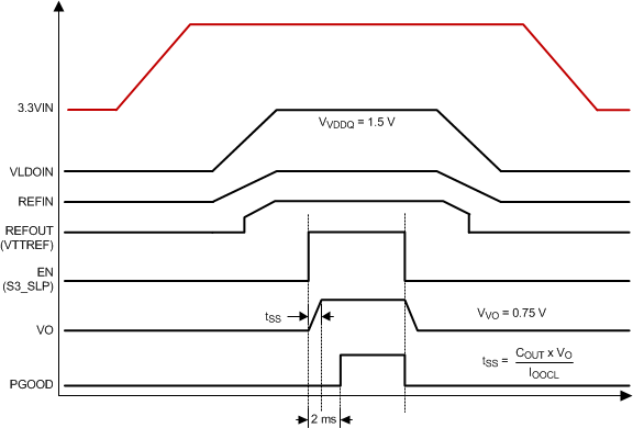
TPS51200-Q1 v08021_lus812.gifFigure 19. Typical Timing Diagram for S3 and Pseudo-S5 Support
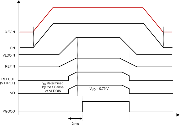
TPS51200-Q1 v08020_lus812.gifFigure 20. Typical Timing Diagram of Tracking Startup and Shutdown