ZHCSI35C November 2009 – April 2018 TPS51200-Q1
PRODUCTION DATA.
- 1 特性
- 2 应用
- 3 说明
- 4 修订历史记录
- 5 Pin Configuration and Functions
- 6 Specifications
- 7 Detailed Description
- 8 Application and Implementation
- 9 Power Supply Recommendations
- 10Layout
- 11器件和文档支持
- 12机械、封装和可订购信息
10.3 Thermal Considerations
Because the TPS51200-Q1 device is a linear regulator, the VO current flows in both source and sink directions, thereby dissipating power from the device. When the device is sourcing current, the voltage difference between VLDOIN and VO times IO (IIO) current becomes the power dissipation as shown in Equation 2.

In this case, if VLDOIN is connected to an alternative power supply lower than the VDDQ voltage, overall power loss can be reduced. For the sink phase, VO voltage is applied across the internal LDO regulator, and the power dissipation, PDISS_SNK can be calculated by Equation 3.

Because the device does not sink and source current at the same time and the IO current may vary rapidly with time, the actual power dissipation must be the time average of the above dissipations over the thermal relaxation duration of the system. Another source of power consumption is the current used for the internal current control circuitry from the VIN supply and the VLDOIN supply. This can be estimated as 5 mW or less during normal operatiing conditions. This power must be effectively dissipated from the package.
Maximum power dissipation allowed by the package is calculated by Equation 4.

where
- TJ(MAX) is 125°C
- TA(MAX) is the maximum ambient temperature in the system
- RθJA is the thermal resistance from junction to ambient
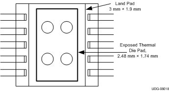
The thermal performance of an LDO depends on the printed circuit board (PCB) layout. The TPS51200-Q1 device is housed in a thermally-enhanced package that has an exposed die pad underneath the body. For improved thermal performance, this die pad must be attached to ground via thermal land on the PCB. This ground trace acts as a both a heatsink and heatspreader. The typical thermal resistance, RθJA, 52.06°C/W, is achieved based on a land pattern of 3 mm × 1,9 mm with four vias (0,33-mm via diameter, the standard thermal via size) without air flow (see Figure 34).
 Figure 34. Recommend Land Pad Pattern for TPS51200-Q1
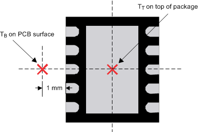
  Figure 35. Package Thermal Measurement
 To further improve the thermal performance of this device, using a larger than recommended thermal land as well as increasing the number of vias helps lower the thermal resistance from junction to thermal pad. The typical thermal resistance from junction to thermal pad, RθJP, is 10.24°C/W (based on the recommend land pad and four standard thermal vias).