ZHCSAF5A OCTOBER 2012 – September 2016 TPS51716
PRODUCTION DATA.
- 1 特性
- 2 应用
- 3 说明
- 4 修订历史记录
- 5 Pin Configuration and Functions
- 6 Specifications
-
7 Detailed Description
- 7.1 Overview
- 7.2 Functional Block Diagram
- 7.3
Feature Description
- 7.3.1 VDDQ Switch Mode Power Supply Control
- 7.3.2 VREF and REFIN, VDDQ Output Voltage
- 7.3.3 Soft-Start and Powergood
- 7.3.4 Power State Control
- 7.3.5 VDDQ Overvoltage and Undervoltage Protection
- 7.3.6 VDDQ Out-of-Bound Operation
- 7.3.7 VDDQ Overcurrent Protection
- 7.3.8 VTT and VTTREF
- 7.3.9 VTT Overcurrent Protection
- 7.3.10 V5IN Undervoltage Lockout (UVLO) Protection
- 7.3.11 Thermal Shutdown
- 7.4 Device Functional Modes
- 8 Application and Implementation
- 9 Power Supply Recommendations
- 10Layout
- 11器件和文档支持
- 12机械、封装和可订购信息
10 Layout
10.1 Layout Guidelines
Certain issues must be considered before designing a layout using the TPS51716.
- VIN capacitor(s), VOUT capacitor(s) and MOSFETs are the power components and should be placed on one side of the PCB (solder side). Other small signal components should be placed on another side (component side). At least one inner system GND plane should be inserted, in order to shield and isolate the small signal traces from noisy power lines.
- All sensitive analog traces and components such as VDDQSNS, VTTSNS, MODE, REFIN, VREF and TRIP should be placed away from high-voltage switching nodes such as SW, DRVL, DRVH or VBST to avoid coupling. Use internal layer(s) as system GND plane(s) and shield feedback trace from power traces and components.
- The DC/DC converter has several high-current loops. The area of these loops should be minimized in order to suppress generating switching noise.
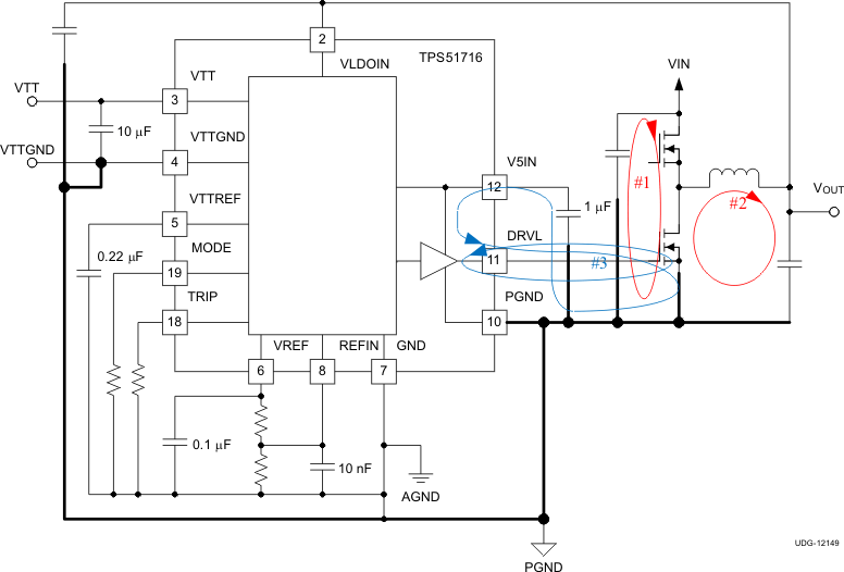
- The most important loop to minimize the area of is the path from the VIN capacitor(s) through the high and low-side MOSFETs, and back to the negative node of the VIN capacitor(s). Connect the negative node of the VIN capacitor(s) and the source of the low-side MOSFET as close as possible. (Refer to loop #1 of Figure 33)
- The second important loop is the path from the low-side MOSFET through inductor and VOUT capacitor(s), and back to source of the low-side MOSFET. Connect the source of the low-side MOSFET and negative node of VOUT capacitor(s) as close as possible. (Refer to loop #2 of Figure 33)
- The third important loop is of gate driving system for the low-side MOSFET. To turn on the low-side MOSFET, high current flows from V5IN capacitor through gate driver and the low-side MOSFET, and back to negative node of the capacitor. To turn off the low-side MOSFET, high current flows from gate of the low-side MOSFET through the gate driver and PGND pin, and back to source of the low-side MOSFET. Connect negative node of V5IN capacitor, source of the low-side MOSFET and PGND pin as close as possible. (Refer to loop #3 of Figure 33)
- Connect negative nodes of the VTTREF output capacitor, VREF capacitor and REFIN capacitor and bottom-side resistance of VREF voltage-divider to GND pin as close as possible. The negative node of the VTT output capacitor(s), VTTGND, GND and PGND pins should be connected to system GND plane near the device as shown in Figure 33.
- Because the TPS51716 controls output voltage referring to voltage across VOUT capacitor, VDDQSNS should be connected to the positive node of VOUT capacitor using different trace from that for VLDOIN. Remember that this sensing potential is the reference voltage of VTTREF. Avoid any noise generative lines. GND pin refers to the negative node of VOUT capacitor.
- Connect the overcurrent setting resistor from TRIP pin to GND pin and make the connections as close as possible to the device to avoid coupling from a high-voltage switching node.
- Connect the frequency and mode setting resistor from MODE pin to GND pin ground, and make the connections as close as possible to the device to avoid coupling from a high-voltage switching node.
- Connections from gate drivers to the respective gate of the high-side or the low-side MOSFET should be as short as possible to reduce stray inductance. Use 0.65 mm (25 mils) or wider trace and via(s) of at least 0.5 mm (20 mils) diameter along this trace.
- The PCB trace defined as SW node, which connects to the source of the high-side MOSFET, the drain of the low-side MOSFET and the high-voltage side of the inductor, should be as short and wide as possible.
- VLDOIN should be connected to VOUT with short and wide traces. An input bypass capacitor should be placed as close as possible to the pin with short and wide connections. The negative node of the capacitor should be connected to system GND plane.
- The output capacitor for VTT should be placed close to the pins with a short and wide connection in order to avoid additional ESR and/or ESL of the trace.
- VTTSNS should be connected to the positive node of the VTT output capacitor(s) using a separate trace from the high-current power line. When remote sensing is required attach the output capacitor(s) at that point. Also, it is recommended to minimize any additional ESR and/or ESL of ground trace between GND pin and the output capacitor(s).
- Consider adding a low pass filter (LPF) at VTTSNS in case the ESR of the VTT output capacitor(s) is larger than 2 mΩ.
- In order to effectively remove heat from the package, prepare a thermal land and solder to the package thermal pad. Wide trace of the component-side copper, connected to this thermal land, helps heat spreading. Numerous vias with a 0.3-mm diameter connected from the thermal land to the internal/solder-side ground plane(s) should be used to help dissipation. The thermal land can be connected to either AGND or PGND but is recommended to be connected to PGND, the system GND plane(s), which has better heat radiation.
10.2 Layout Example
 Figure 33. DC/DC Converter Ground System