ZHCSJ77F December   2010  – December 2018 TPS51916

PRODUCTION DATA.  

  1. 特性
  2. 应用
  3. 说明
    1.     简化应用
  4. 修订历史记录
  5. Pin Configuration and Functions
    1.     Pin Functions
  6. Specifications
    1. 6.1 Absolute Maximum Ratings
    2. 6.2 ESD Ratings
    3. 6.3 Recommended Operating Conditions
    4. 6.4 Thermal Information
    5. 6.5 Electrical Characteristics
    6. 6.6 Typical Characteristics
  7. Detailed Description
    1. 7.1 Overview
    2. 7.2 Functional Block Diagram
    3. 7.3 Feature Description
      1. 7.3.1  VDDQ Switch Mode Power Supply Control
      2. 7.3.2  VREF and REFIN, VDDQ Output Voltage
      3. 7.3.3  Soft-Start and Powergood
      4. 7.3.4  Power State Control
      5. 7.3.5  Discharge Control
      6. 7.3.6  VTT and VTTREF
      7. 7.3.7  VDDQ Overvoltage and Undervoltage Protection
      8. 7.3.8  VDDQ Out-of-Bound Operation
      9. 7.3.9  VDDQ Overcurrent Protection
      10. 7.3.10 VTT Overcurrent Protection
      11. 7.3.11 V5IN Undervoltage Lockout Protection
      12. 7.3.12 Thermal Shutdown
    4. 7.4 Device Functional Modes
      1. 7.4.1 MODE Pin Configuration
      2. 7.4.2 D-CAP™ Mode
    5. 7.5 D-CAP2™ Mode Operation
  8. Application and Implementation
    1. 8.1 Application Information
      1. 8.1.1 DDR3, D-CAP™ 400-kHz Application with Tracking Discharge
        1. 8.1.1.1 Design Requirements
        2. 8.1.1.2 Detailed Design Procedure
          1. 8.1.1.2.1 1. Determine the value of R1 AND R2
          2. 8.1.1.2.2 2. Choose the inductor
          3. 8.1.1.2.3 3. Choose the OCL setting resistance, RTRIP
          4. 8.1.1.2.4 Choose the output capacitors
        3. 8.1.1.3 Application Curves
      2. 8.1.2 DDR3, DCAP-2 500-kHz Application, with Tracking Discharge
        1. 8.1.2.1 Design Requirements
        2. 8.1.2.2 Detailed Design Procedure
          1. 8.1.2.2.1 Select Mode and Switching Frequency
          2. 8.1.2.2.2 Determine output capacitance
        3. 8.1.2.3 Application Curves
  9. Power Supply Recommendations
  10. 10Layout
    1. 10.1 Layout Guidelines
    2. 10.2 Layout Example
  11. 11器件和文档支持
    1. 11.1 接收文档更新通知
    2. 11.2 社区资源
    3. 11.3 商标
    4. 11.4 静电放电警告
    5. 11.5 术语表
  12. 12机械、封装和可订购信息

封装选项

机械数据 (封装 | 引脚)
散热焊盘机械数据 (封装 | 引脚)
订购信息

1. Determine the value of R1 AND R2

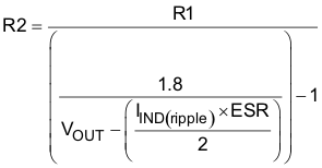
The output voltage is determined by the value of the voltage-divider resistor, R1 and R2 as shown in Figure 36. R1 is connected between VREF and REFIN pins, and R2 is connected between the REFIN pin and GND. Setting R1 as 10-kΩ is a good starting point. Determine R2 using Equation 6.

Equation 6. TPS51916 q_r2_lusab9.gif