ZHCSED1A November   2015  – November 2015 TPS53317A

PRODUCTION DATA.  

  1. 特性
  2. 应用
  3. 说明
  4. 修订历史记录
  5. Pin Configuration and Functions
  6. Specifications
    1. 6.1 Absolute Maximum Ratings
    2. 6.2 ESD Ratings
    3. 6.3 Recommended Operating Conditions
    4. 6.4 Thermal Information
    5. 6.5 Electrical Characteristics
    6. 6.6 Typical Characteristics
  7. Detailed Description
    1. 7.1 Overview
    2. 7.2 Functional Block Diagram
    3. 7.3 Feature Description
      1. 7.3.1 PWM Operation
      2. 7.3.2 PWM Frequency and Adaptive On-Time Control
      3. 7.3.3 Light-Load Power Saving Features
      4. 7.3.4 Power Sequences
        1. 7.3.4.1 Non-Tracking Startup
        2. 7.3.4.2 Tracking Startup
      5. 7.3.5 Protection Features
        1. 7.3.5.1 5-V Undervoltage Protection (UVLO)
        2. 7.3.5.2 Power Good Signals
        3. 7.3.5.3 Output Overvoltage Protection (OVP)
        4. 7.3.5.4 Output Undervoltage Protection (UVP)
        5. 7.3.5.5 Overcurrent Protection
          1. 7.3.5.5.1 Overcurrent Limit
          2. 7.3.5.5.2 Negative OCL
      6. 7.3.6 Thermal Protection
    4. 7.4 Device Functional Modes
      1. 7.4.1 Non-Droop Configuration
      2. 7.4.2 Droop Configuration
  8. Application and Implementation
    1. 8.1 Application Information
    2. 8.2 Typical Applications
      1. 8.2.1 DDR4 SDRAM Application
        1. 8.2.1.1 Design Requirements
        2. 8.2.1.2 Detailed Design Procedure
          1. 8.2.1.2.1 Step 1. Determine Configuration
          2. 8.2.1.2.2 Step 2. Select Inductor
          3. 8.2.1.2.3 Step 3. Determine Output Capacitance
          4. 8.2.1.2.4 Step 4. Input Capacitance
          5. 8.2.1.2.5 Step 5. Compensation Network
          6. 8.2.1.2.6 Peripheral Component Selection
        3. 8.2.1.3 Application Curves
      2. 8.2.2 DDR3 SDRAM Application
        1. 8.2.2.1 Design Requirements
      3. 8.2.3 Non-Tracking Point-of-Load (POL) Application
        1. 8.2.3.1 Design Requirements
        2. 8.2.3.2 Application Curves
  9. Power Supply Recommendations
  10. 10Layout
    1. 10.1 Layout Guidelines
    2. 10.2 Layout Example
  11. 11器件和文档支持
    1. 11.1 社区资源
    2. 11.2 商标
    3. 11.3 静电放电警告
    4. 11.4 Glossary
  12. 12机械、封装和可订购信息

封装选项

机械数据 (封装 | 引脚)
散热焊盘机械数据 (封装 | 引脚)
订购信息

5 Pin Configuration and Functions

RGB Package
20-Pin VFQN
Top View
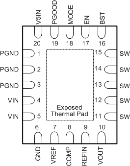
TPS53317A pinout_rgb_20x_slusak4.gif

Pin Functions

PIN I/O(1) DESCRIPTION
NAME NO.
BST 16 I Power supply for internal high-side gate driver. Connect a 0.1-µF bootstrap capacitor between this pin and the SW pin. Include a series boot resistor when the voltage spike on switching node is above 7 V.
COMP 8 O Connect an R-C-C network between this pin and VREF for loop compensation.
EN 17 I Enable pin (3.3-V logic compatible).
GND 6 Analog ground.
MODE 18 I Allows selection of different operation modes. (See Table 1)
PGND 1 G Power ground.
2
3
PGOOD 19 O Open drain power good output. Connect pullup resistor.
REFIN 9 I External tracking reference input. Apply voltage between 0.45 V to 2.0 V. For non-tracking mode, connect REFIN to VREF via resistor divider.
SW 11 I/O Switching node output.
12
13
14
15
V5IN 20 I 5-V power supply for analog circuits and gate drive.
VIN 4 I Power supply input pin.
5
VOUT 10 I Output voltage monitor input pin.
VREF 7 O 2.0-V reference output. Connect a ceramic capacitor with a value of 0.22-µF or greater between this pin and GND.
(1) I = Input, O = Output, G = Ground