ZHCS922C May 2012 – October 2015 TPS54140A
PRODUCTION DATA.
- 1 特性
- 2 应用范围
- 3 说明
- 4 修订历史记录
- 5 Pin Configuration and Functions
- 6 Specifications
-
7 Detailed Description
- 7.1 Overview
- 7.2 Functional Block Diagram
- 7.3
Feature Description
- 7.3.1 Fixed Frequency PWM Control
- 7.3.2 Slope Compensation Output Current
- 7.3.3 Pulse Skip Eco-mode
- 7.3.4 Bootstrap Voltage (BOOT)
- 7.3.5 Low Dropout Operation
- 7.3.6 Error Amplifier
- 7.3.7 Voltage Reference
- 7.3.8 Overload Recovery Circuit
- 7.3.9 Overcurrent Protection and Frequency Shift
- 7.3.10 Power Good (PWRGD Pin)
- 7.3.11 Overvoltage Transient Protection
- 7.3.12 Thermal Shutdown
- 7.4 Device Functional Modes
-
8 Application and Implementation
- 8.1 Application Information
- 8.2
Typical Application
- 8.2.1 Design Requirements
- 8.2.2
Detailed Design Procedure
- 8.2.2.1 Selecting the Switching Frequency
- 8.2.2.2 Output Inductor Selection (LO)
- 8.2.2.3 Output Capacitor
- 8.2.2.4 Catch Diode
- 8.2.2.5 Input Capacitor
- 8.2.2.6 Slow Start Capacitor
- 8.2.2.7 Bootstrap Capacitor Selection
- 8.2.2.8 Undervoltage Lock Out Set Point
- 8.2.2.9 Output Voltage and Feedback Resistors Selection
- 8.2.2.10 Compensation
- 8.2.3 Application Curves
- 8.3 System Examples
- 9 Power Supply Recommendations
- 10Layout
- 11器件和文档支持
- 12机械、封装和可订购信息
封装选项
机械数据 (封装 | 引脚)
散热焊盘机械数据 (封装 | 引脚)
订购信息
6 Specifications
6.1 Absolute Maximum Ratings(1)
Over operating temperature range (unless otherwise noted).| MIN | MAX | UNIT | ||
|---|---|---|---|---|
| Input voltage | VIN | –0.3 | 47 | V |
| EN(2) | –0.3 | 5 | ||
| BOOT | 55 | |||
| VSENSE | –0.3 | 3 | ||
| COMP | –0.3 | 3 | ||
| PWRGD | –0.3 | 6 | ||
| SS/TR | –0.3 | 3 | ||
| RT/CLK | –0.3 | 3.6 | ||
| Output voltage | PH–BOOT | 8 | V | |
| PH | –0.6 | 47 | ||
| PH, 10-ns Transient | –2 | 47 | ||
| Voltage Difference | PAD to GND | ±200 | mV | |
| Source current | EN | 100 | μA | |
| BOOT | 100 | mA | ||
| VSENSE | 10 | μA | ||
| PH | Current Limit | A | ||
| RT/CLK | 100 | μA | ||
| Sink current | VIN | Current Limit | A | |
| COMP | 100 | μA | ||
| PWRGD | 10 | mA | ||
| SS/TR | 200 | μA | ||
| Operating junction temperature | –40 | 150 | °C | |
| Storage temperature | –65 | 150 | °C | |
(1) Stresses beyond those listed under absolute maximum ratings may cause permanent damage to the device. These are stress ratings only and functional operation of the device at these or any other conditions beyond those indicated under recommended operating conditions is not implied. Exposure to absolute-maximum-rated conditions for extended periods may affect device reliability.
(2) See the Enable and Adjusting Undervoltage Lockout section of this data sheet for details.
6.2 ESD Ratings
| VALUE | UNIT | |||
|---|---|---|---|---|
| DRC package (VSON) | ||||
| V(ESD) | Electrostatic discharge | Human-body model (HBM), per ANSI/ESDA/JEDEC JS-001(1) | ±2000 | V |
| Charged-device model (CDM), per JEDEC specification JESD22-C101(2) | ±500 | |||
| DGQ package (MSOP) | ||||
| V(ESD) | Electrostatic discharge | Human-body model (HBM), per ANSI/ESDA/JEDEC JS-001(1) | ±2000 | V |
| Charged-device model (CDM), per JEDEC specification JESD22-C101(2) | ±500 | |||
(1) JEDEC document JEP155 states that 500-V HBM allows safe manufacturing with a standard ESD control process. Manufacturing with less than 500-V HBM is possible if necessary precautions are taken.
(2) JEDEC document JEP157 states that 250-V CDM allows safe manufacturing with a standard ESD control process. Manufacturing with less than 250-V CDM is possible if necessary precautions are taken.
6.3 Recommended Operating Conditions
over operating free-air temperature range (unless otherwise noted)| MIN | MAX | UNIT | ||
|---|---|---|---|---|
| VIN | Supply input voltage range | 3.5 | 42 | V |
| VO | Output voltage range | 0.8 | 39 | V |
6.4 Thermal Information
| THERMAL METRIC(1) | TPS54140A | UNIT | ||
|---|---|---|---|---|
| DGQ (MSOP) | DRC (VSON) | |||
| 10 PINS | 10 PINS | |||
| RθJA | Junction-to-ambient thermal resistance (standard board) | 52.3 | 45.1 | °C/W |
| RθJC(top) | Junction-to-case (top) thermal resistance | 46.3 | 51.9 | °C/W |
| RθJB | Junction-to-board thermal resistance | 33 | 20.5 | °C/W |
| ψJT | Junction-to-top characterization parameter | 1.6 | 0.8 | °C/W |
| ψJB | Junction-to-board characterization parameter | 32.7 | 20.7 | °C/W |
| RθJC(bot) | Junction-to-case (bottom) thermal resistance | 5.9 | 5.1 | °C/W |
(1) For more information about traditional and new thermal metrics, see the Semiconductor and IC Package Thermal Metrics application report, SPRA953.
6.5 Electrical Characteristics
TJ = –40°C to 150°C, VIN = 3.5 to 42 V (unless otherwise noted)6.6 Typical Characteristics
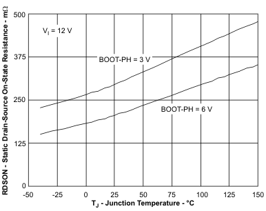 Figure 1. ON Resistance vs Junction Temperature
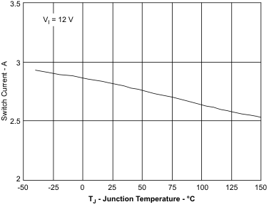 Figure 3. Switch Current Limit vs Junction Temperature
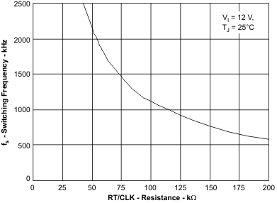 Figure 5. Switching Frequency vs RT/CLK Resistance High Frequency Range
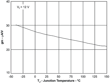 Figure 7. EA Transconductance During Slow Start vs Junction Temperature
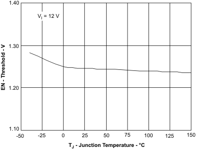 Figure 9. EN Pin Voltage vs Junction Temperature
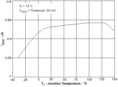 Figure 11. EN Pin Current vs Junction Temperature
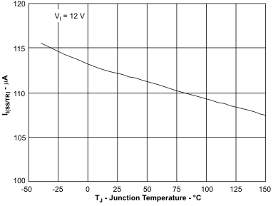 Figure 13. SS/TR Discharge Current vs Junction Temperature
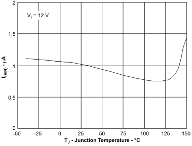 Figure 15. Shutdown Supply Current vs Junction Temperature
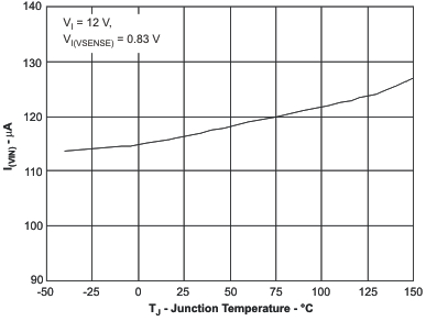 Figure 17. VIN Supply Current vs Junction Temperature
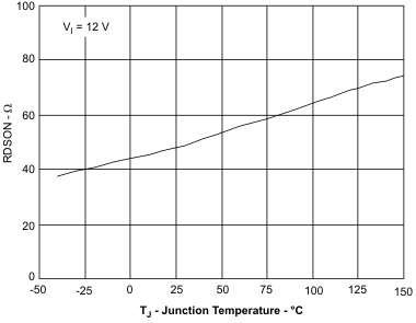 Figure 19. PWRGD ON Resistance vs Junction Temperature
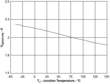 Figure 21. BOOT-PH UVLO vs Junction Temperature
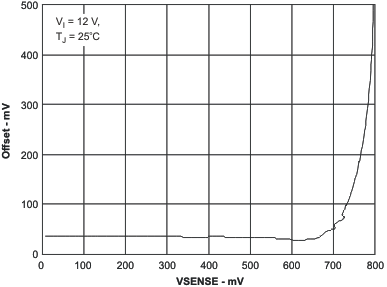 Figure 23. SS/TR to VSENSE Offset vs VSENSE
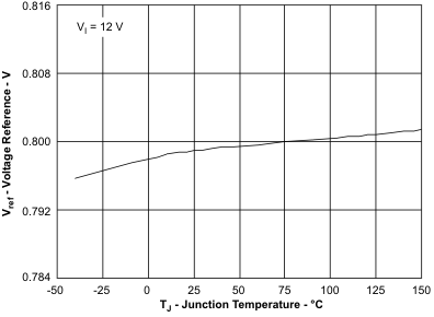 Figure 2. Voltage Reference vs Junction Temperature
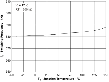 Figure 4. Switching Frequency vs Junction Temperature
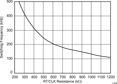 Figure 6. Switching Frequency vs RT/CLK Resistance Low Frequency Range
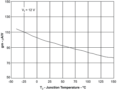 Figure 8. EA Transconductance vs Junction Temperature
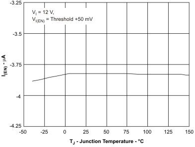 Figure 10. EN Pin Current vs Junction Temperature
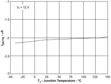 Figure 12. SS/TR Charge Current vs Junction Temperature
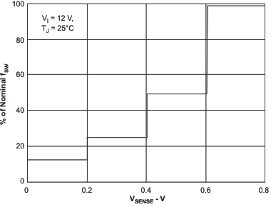 Figure 14. Switching Frequency vs VSENSE
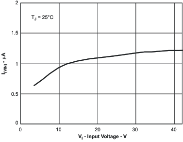 Figure 16. Shutdown Supply Current vs Input Voltage (Vin)
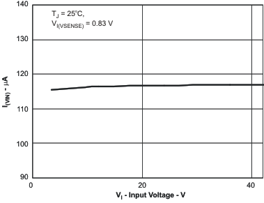 Figure 18. VIN Supply Current vs Input Voltage
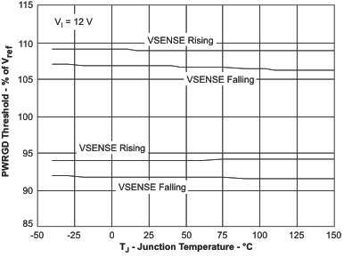 Figure 20. PWRGD Threshold vs Junction Temperature
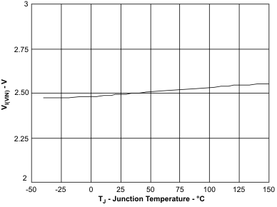 Figure 22. Input Voltage (UVLO) vs Junction Temperature
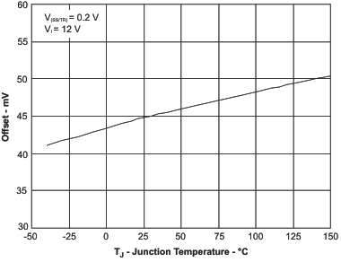 Figure 24. SS/TR to VSENSE Offset vs Temperature