ZHCSJ36 November 2018 TPS543C20A
PRODUCTION DATA.
- 1 特性
- 2 应用
- 3 说明
- 4 修订历史记录
- 5 Device Comparison Table
- 6 Pin Configuration and Functions
- 7 Specifications
-
8 Detailed Description
- 8.1 Overview
- 8.2 Functional Block Diagram
- 8.3 Feature Description
- 8.4
Device Functional Modes
- 8.4.1 Soft-Start Operation
- 8.4.2 Input and VDD Undervoltage Lockout (UVLO) Protection
- 8.4.3 Power Good and Enable
- 8.4.4 Voltage Reference
- 8.4.5 Prebiased Output Start-up
- 8.4.6 Internal Ramp Generator
- 8.4.7 Switching Frequency
- 8.4.8 Clock Sync Point Selection
- 8.4.9 Synchronization and Stackable Configuration
- 8.4.10 Dual-Phase Stackable Configurations
- 8.4.11 Operation Mode
- 8.4.12 API/Body Brake
- 8.4.13 Sense and Overcurrent Protection
- 8.4.14 Output Overvoltage and Undervoltage Protection
- 8.4.15 Overtemperature Protection
- 8.4.16 RSP/RSN Remote Sense Function
- 8.4.17 Current Sharing
- 8.4.18 Loss of Synchronization
-
9 Application and Implementation
- 9.1 Application Information
- 9.2
Typical Application: TPS543C20A Stand-alone Device
- 9.2.1 Design Requirements
- 9.2.2 Detailed Design Procedure
- 9.2.3 Application Curves
- 9.3 System Example
- 10Power Supply Recommendations
- 11Layout
- 12器件和文档支持
- 13机械、封装和可订购信息
9.3.1.1 Application Curves
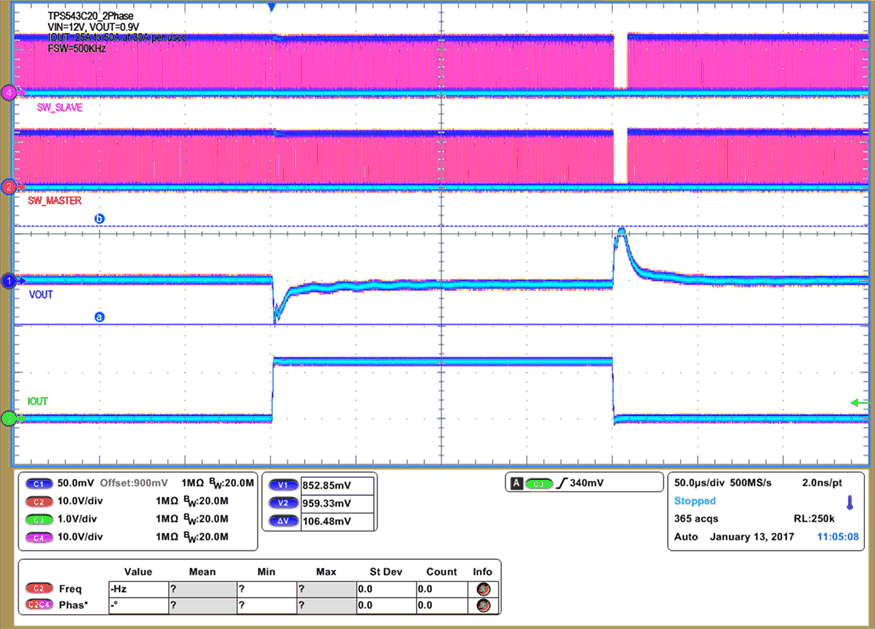 Figure 34. Transient Response of 0.9-V Output at 12 VIN, Transient is 25 A to 50 A, Step is 25 A at 30 A/μs
 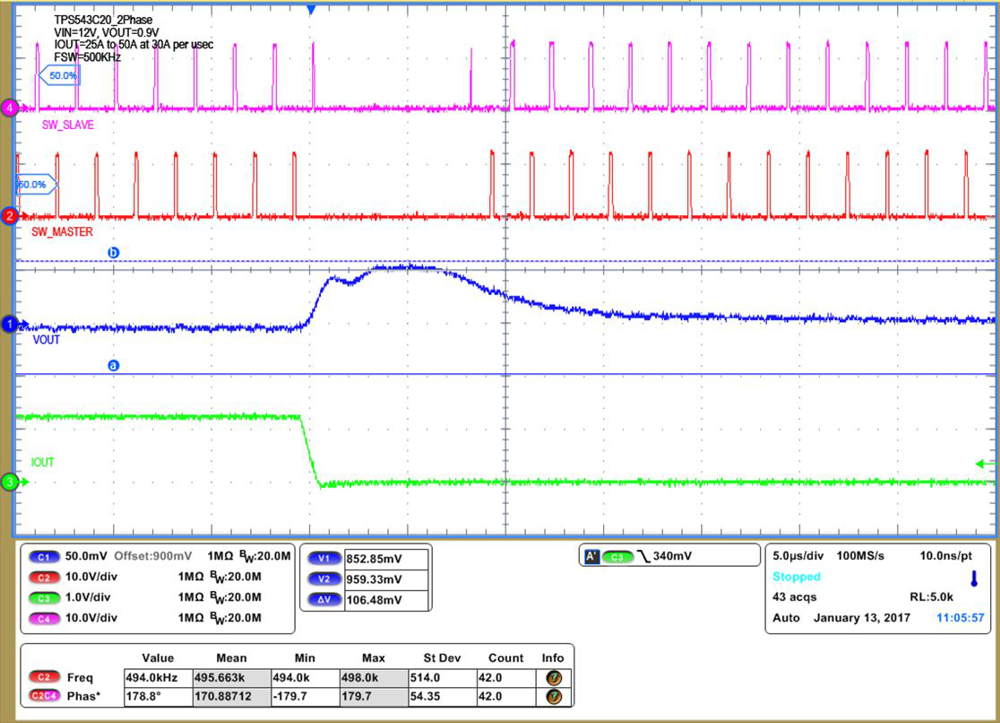 Figure 36. Transient Response of 50-A to 25-A Load
at 30 A/μs Fall
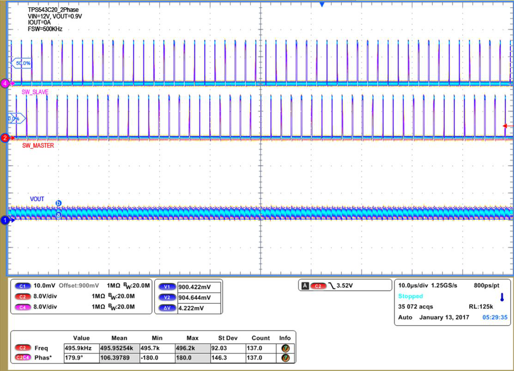 Figure 38. Output Ripple and SW Node
of 0.9-V Output at 12 VIN, 0-A Output
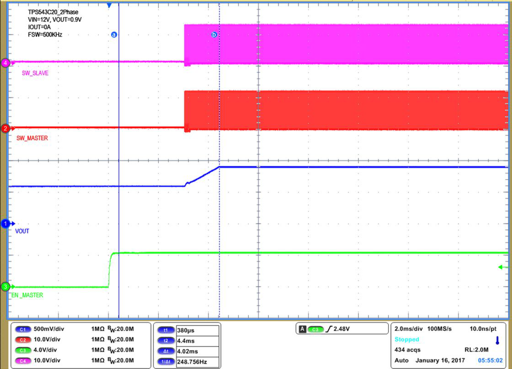 Figure 40. 0.6-V Pre-Bias Start Up From Enable,
0.9-V Output at 12 VIN, 0-A Output
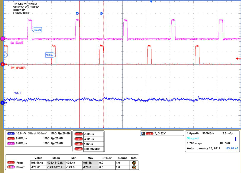 Figure 42. Master-Slave 180° Synchronization
 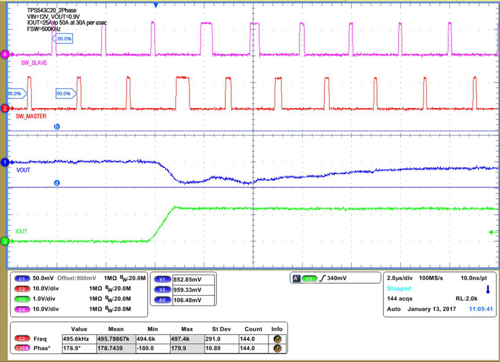 Figure 35. Transient Response of 25-A to 50-A Load
at 30 A/μs Rise
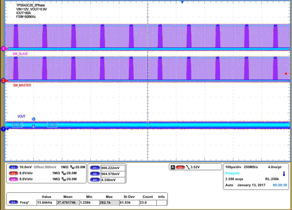 Figure 37. Output Ripple and SW Node
of 0.9-V Output at 12 VIN, -A Output
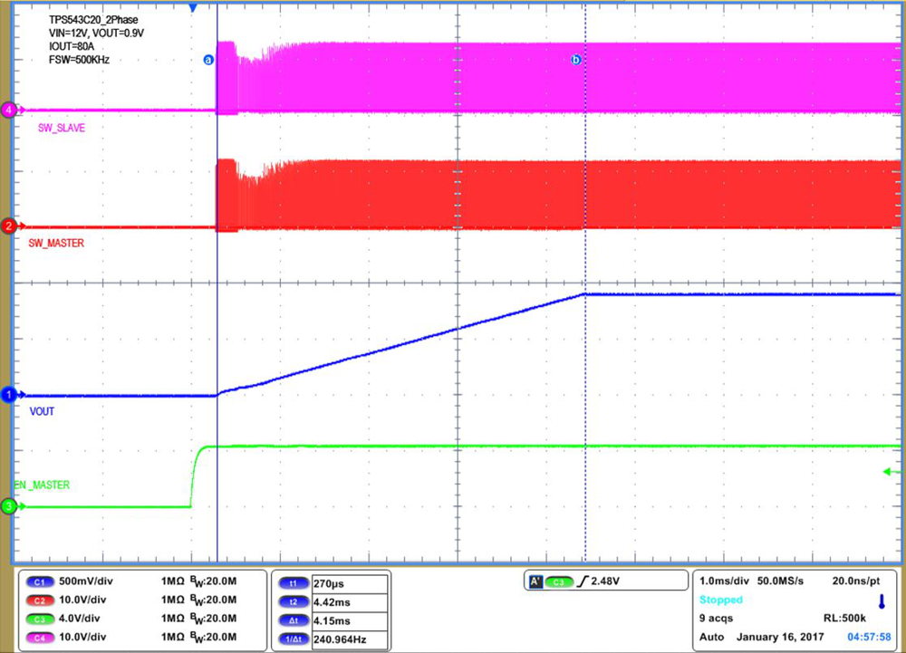 Figure 39. Start up from Enable,
0.9-V Output at 12 VIN, 80-A Output
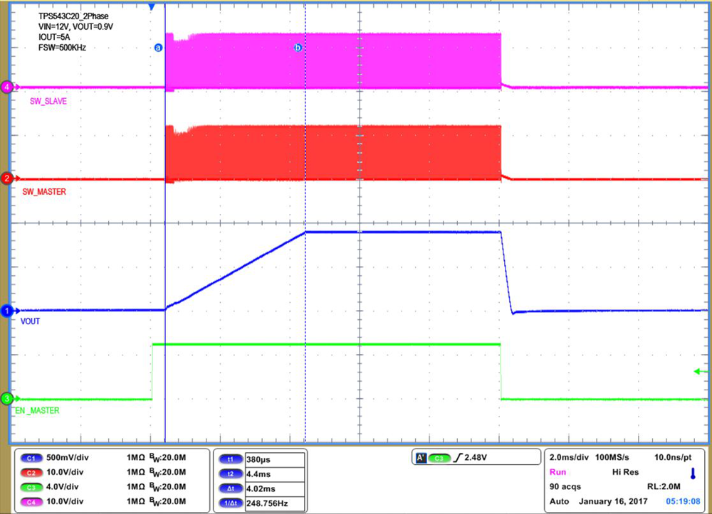 Figure 41. Output Voltage Start-up and Shutdown,
0.9-V Output at 12 VIN, 5-A Output