ZHCSJ36 November 2018 TPS543C20A
PRODUCTION DATA.
- 1 特性
- 2 应用
- 3 说明
- 4 修订历史记录
- 5 Device Comparison Table
- 6 Pin Configuration and Functions
- 7 Specifications
-
8 Detailed Description
- 8.1 Overview
- 8.2 Functional Block Diagram
- 8.3 Feature Description
- 8.4
Device Functional Modes
- 8.4.1 Soft-Start Operation
- 8.4.2 Input and VDD Undervoltage Lockout (UVLO) Protection
- 8.4.3 Power Good and Enable
- 8.4.4 Voltage Reference
- 8.4.5 Prebiased Output Start-up
- 8.4.6 Internal Ramp Generator
- 8.4.7 Switching Frequency
- 8.4.8 Clock Sync Point Selection
- 8.4.9 Synchronization and Stackable Configuration
- 8.4.10 Dual-Phase Stackable Configurations
- 8.4.11 Operation Mode
- 8.4.12 API/Body Brake
- 8.4.13 Sense and Overcurrent Protection
- 8.4.14 Output Overvoltage and Undervoltage Protection
- 8.4.15 Overtemperature Protection
- 8.4.16 RSP/RSN Remote Sense Function
- 8.4.17 Current Sharing
- 8.4.18 Loss of Synchronization
-
9 Application and Implementation
- 9.1 Application Information
- 9.2
Typical Application: TPS543C20A Stand-alone Device
- 9.2.1 Design Requirements
- 9.2.2 Detailed Design Procedure
- 9.2.3 Application Curves
- 9.3 System Example
- 10Power Supply Recommendations
- 11Layout
- 12器件和文档支持
- 13机械、封装和可订购信息
11.3 Package Size, Efficiency and Thermal Performance
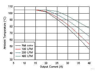
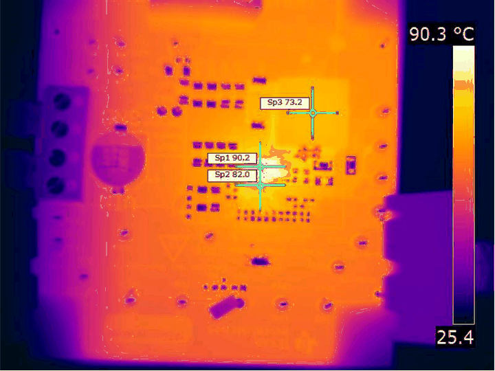
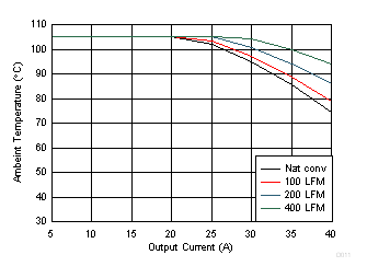
The TPS543C20A device is available in a 5 mm × 7 mm, QFN package with 40 power and I/O pins. It employs TI proprietary MCM packaging technology with thermal pad. With a properly designed system layout, applications achieve optimized safe operating area (SOA) performance. The curves shown in and are based on the orderable evaluation module design.

| VIN = 12 V | VOUT = 5 V | 500 kHz |
 Figure 46. Thermal Image at 1.0-V Output at 12 VIN, 40-A Output, at 25°C Ambient
1.
Figure 45. Safe Operating Area | VIN = 12 V | VOUT = 1 V | 500 kHz |
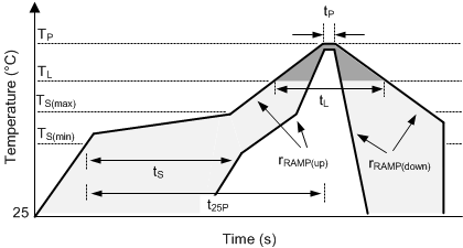
 Figure 47. Recommended Reflow Oven Thermal Profile
 Table 7. Recommended Thermal Profile Parameters
| PARAMETER | MIN | TYP | MAX | UNIT | ||||
|---|---|---|---|---|---|---|---|---|
| RAMP UP AND RAMP DOWN | ||||||||
| rRAMP(up) | Average ramp-up rate, TS(MAX) to TP | 3 | °C/s | |||||
| rRAMP(down) | Average ramp-down rate, TP to TS(MAX) | 6 | °C/s | |||||
| PRE-HEAT | ||||||||
| TS | Pre-heat temperature | 150 | 200 | °C | ||||
| tS | Pre-heat time, TS(min) to TS(max) | 60 | 180 | s | ||||
| REFLOW | ||||||||
| TL | Liquidus temperature | 217 | °C | |||||
| TP | Peak temperature | 260 | °C | |||||
| tL | Time maintained above liquidus temperature, TL | 60 | 150 | s | ||||
| tP | Time maintained within 5°C of peak temperature, TP | 20 | 40 | s | ||||
| t25P | Total time from 25°C of peak temperature, TP | 480 | s | |||||