ZHCSE52B September 2015 – May 2019 TPS57140-EP
PRODUCTION DATA.
- 1 特性
- 2 应用范围
- 3 说明
- 4 修订历史记录
- 5 Pin Configuration and Functions
- 6 Specifications
-
7 Detailed Description
- 7.1 Overview
- 7.2 Functional Block Diagram
- 7.3
Feature Description
- 7.3.1 Fixed Frequency PWM Control
- 7.3.2 Slope-Compensation Output Current
- 7.3.3 Bootstrap Voltage (Boot)
- 7.3.4 Low-Dropout Operation
- 7.3.5 Error Amplifier
- 7.3.6 Voltage Reference
- 7.3.7 Adjusting the Output Voltage
- 7.3.8 Enable and Adjusting UVLO
- 7.3.9 Slow-Start or Tracking Pin (SS/TR)
- 7.3.10 Overload Recovery Circuit
- 7.3.11 Constant Switching Frequency and Timing Resistor (RT/CLK Pin)
- 7.3.12 Overcurrent Protection and Frequency Shift
- 7.3.13 Selecting the Switching Frequency
- 7.3.14 How to Interface to RT/CLK Pin
- 7.3.15 Power Good (PWRGD Pin)
- 7.3.16 Overvoltage Transient Protection (OVTP)
- 7.3.17 Thermal Shutdown
- 7.3.18 Small-Signal Model for Loop Response
- 7.3.19 Simple Small-Signal Model for Peak-Current-Mode Control
- 7.3.20 Small-Signal Model for Frequency Compensation
- 7.4 Device Functional Modes
-
8 Application and Implementation
- 8.1 Application Information
- 8.2
Typical Application
- 8.2.1 Design Requirements
- 8.2.2
Detailed Design Procedure
- 8.2.2.1 Selecting the Switching Frequency
- 8.2.2.2 Output Inductor Selection (LO)
- 8.2.2.3 Output Capacitor
- 8.2.2.4 Catch Diode
- 8.2.2.5 Input Capacitor
- 8.2.2.6 Slow-Start Capacitor
- 8.2.2.7 Bootstrap Capacitor Selection
- 8.2.2.8 UVLO Set Point
- 8.2.2.9 Output Voltage and Feedback Resistors Selection
- 8.2.2.10 Compensation
- 8.2.3 Application Curves
- 9 Power Supply Recommendations
- 10Layout
- 11器件和文档支持
- 12机械、封装和可订购信息
7.4.1 Sequencing
The designer can implement many of the common power-supply sequencing methods using the SS/TR, EN, and PWRGD pins. Implement the sequential method using an open-drain output of a power-on-reset pin of another device. Figure 43 shows the sequential method using two TPS57140-EP devices. The power-good pin connects to the EN pin on the TPS57140-EP, which enables the second power supply when the primary supply reaches regulation. If needed, a 1-nF ceramic capacitor on the EN pin of the second power supply provides a 1-ms start-up delay. Figure 44 shows the results of Figure 43.
Figure 45 shows a method for a ratiometric start-up sequence by connecting the SS/TR pins together. The regulator outputs ramp up and reach regulation at the same time. When calculating the slow-start time, the pullup current source must be doubled in Equation 6. Figure 46 shows the results of Figure 45.
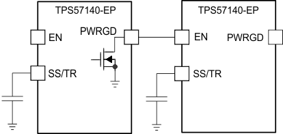
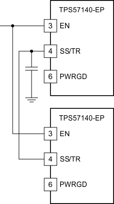
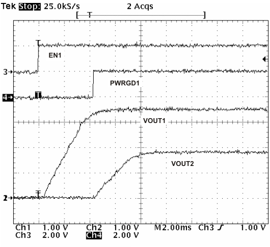
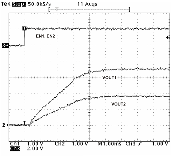
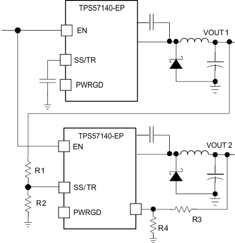 Figure 47. Schematic for Ratiometric and Simultaneous Start-Up Sequence
 The designer can implement ratiometric and simultaneous power-supply sequencing by connecting the resistor network of R1 and R2 shown in Figure 47 to the output of the power supply that requires tracking, or to another voltage reference source. Using Equation 24 and Equation 25, calculate values for the tracking resistors to initiate the Vout2 slightly before, after, or at the same time as Vout1. Equation 26 is the voltage difference between Vout1 and Vout2 at 95% of nominal output regulation.
The deltaV variable is 0 V for simultaneous sequencing. To minimize the effect of the inherent SS/TR-to-VSENSE offset (Vssoffset) in the slow-start circuit and the offset created by the pullup current source (Iss) and tracking resistors, the equations include Vssoffset and Iss as variables.
To design a ratiometric start-up in which the Vout2 voltage is slightly greater than the Vout1 voltage when Vout2 reaches regulation, use a negative number in Equation 24 through Equation 26 for deltaV. Equation 26 results in a positive number for applications in which Vout2 is slightly lower than Vout1 when Vout2 regulation is achieved.
Because the SS/TR pin must be below 40 mV before starting after an EN, UVLO, or thermal shutdown fault, a design requires careful selection of the tracking resistors to ensure the device restarts after a fault. Make sure the calculated R1 value from Equation 24 is greater than the value calculated in Equation 27 to ensure the device can recover from a fault.
As the SS/TR voltage becomes more than 85% of the nominal reference voltage, Vssoffset becomes larger as the slow-start circuits gradually hand off the regulation reference to the internal voltage reference. The SS/TR pin voltage must be greater than 1.3 V for a complete handoff to the internal voltage reference as shown in Figure 24.


