ZHCSFA0 June 2016 TPS61021A
PRODUCTION DATA.
- 1 特性
- 2 应用
- 3 说明
- 4 修订历史记录
- 5 Pin Configuration and Functions
- 6 Specifications
- 7 Detailed Description
- 8 Application and Implementation
- 9 Power Supply Recommendations
- 10Layout
- 11器件和文档支持
- 12机械、封装和可订购信息
8 Application and Implementation
NOTE
Information in the following applications sections is not part of the TI component specification, and TI does not warrant its accuracy or completeness. TI’s customers are responsible for determining suitability of components for their purposes. Customers should validate and test their design implementation to confirm system functionality.
8.1 Application Information
The TPS61021A is a synchronous boost converter designed to operate from an input voltage supply range between 0.5 V and 4.4 V with 3-A valley switch current limit. The TPS61021A typically operates at a quasi-constant 2-MHz frequency pulse width modulation (PWM) at moderate to heavy load currents when the input voltage is above 1.5 V. The switching frequency changes to 1-MHz gradually with the input voltage changing from 1.5 V to 1 V to get better efficiency and high step-up ratio. At light load currents, the TPS61021A converter operates in power-save mode with pulse frequency modulation (PFM) to achieve high efficiency over the entire load current range.
8.2 Typical Application
The TPS61021A provides a power supply solution for portable or smart devices powered by batteries or super-capacitors. With 3-A switch current capability, the TPS61021A can output 3.3 V and 1.5 A from two alkaline batteries in series even if the battery voltage is down to 1.8 V.
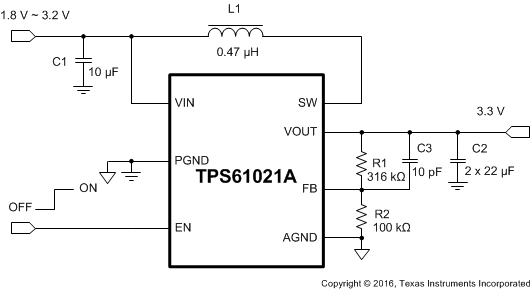 Figure 11. 2-Cell Alkaline Battery to 3.3-V Boost Converter
8.2.1 Design Requirements
The design parameters are listed in Table 1.
Table 1. Design Parameters
| PARAMETERS | VALUES |
|---|---|
| Input voltage | 1.8 V to 3.2 V |
| Output voltage | 3.3 V |
| Output current | 1.5 A |
| Output voltage ripple | ±50 mV |
8.2.2 Detailed Design Procedure
8.2.2.1 Setting the Output Voltage
The output voltage is set by an external resistor divider (R1, R2 in Figure 11). When the output voltage is regulated, the typical voltage at the FB pin is VREF. Thus the resistor divider is determined by Equation 4.

Where:
VOUT is the regulated output voltage
VREF is the internal reference voltage at the FB pin
For best accuracy, R2 should be kept smaller than 400 kΩ to ensure the current flowing through R2 is at least 100 times larger than the FB pin leakage current. Changing R2 towards a lower value increases the immunity against noise injection. Changing the R2 towards a higher value reduces the quiescent current for achieving highest efficiency at low load currents.
8.2.2.2 Inductor Selection
Because the selection of the inductor affects steady state operation, transient behavior, and loop stability, the inductor is the most important component in power regulator design. There are three important inductor specifications, inductor value, saturation current, and dc resistance (DCR).
The TPS61021A is designed to work with inductor values between 0.33 µH and 1.0 µH. Follow Equation 5 to Equation 7 to calculate the inductor’s peak current for the application. To calculate the current in the worst case, use the minimum input voltage, maximum output voltage, and maximum load current of the application. To have enough design margins, choose the inductor value with -30% tolerances, and low power-conversion efficiency for the calculation.
In a boost regulator, the inductor dc current can be calculated by Equation 5.

Where:
VOUT is the output voltage of the boost converter
IOUT is the output current of the boost converter
VIN is the input voltage of the boost converter
η is the power conversion efficiency, use 90% for most applications
The inductor ripple current is calculated by Equation 6.

Where:
D is the duty cycle, which can be calculated by Equation 2
L is the inductance value of the inductor
fSW is the switching frequency
VIN is the input voltage of the boost converter
Therefore, the inductor peak current is calculated by Equation 7.

Normally, it is advisable to work with an inductor peak-to-peak current of less than 40% of the average inductor current for maximum output current. A smaller ripple from a larger valued inductor reduces the magnetic hysteresis losses in the inductor and EMI. But in the same way, load transient response time is increased. The inductor’s saturation current must be higher than the calculated peak inductor current. Table 2 lists the recommended inductors for the TPS61021A.
Table 2. Recommended Inductors for the TPS61021A
| PART NUMBER | L(µH) | DCR MAX (mΩ) | SATURATION CURRENT (A) | SIZE (LxWxH) | VENDOR(1) |
|---|---|---|---|---|---|
| XFL4015-471ME | 0.47 | 8.36 | 6.6 | 4.0×4.0×1.5 | Coilcraft |
| 744383360047 | 0.47 | 22 | 8.0 | 3.0x3.0x2.0 | Wurth Elecktronik |
| DFE252012P-R47M | 0.47 | 27 | 5.7 | 2.5×2.0×1.2 | Toko |
| XFL4020-102ME | 1.0 | 11.9 | 5.4 | 4.0×4.0×2.1 | Coilcraft |
8.2.2.3 Output Capacitor Selection
The output capacitor is mainly selected to meet the requirements for output ripple and loop stability. The ripple voltage is related to the capacitor’s capacitance and its equivalent series resistance (ESR). Assuming a ceramic capacitor with zero ESR, the minimum capacitance needed for a given ripple voltage can be calculated by Equation 8.

Where:
DMAX is the maximum switching duty cycle
VRIPPLE is the peak to peak output ripple voltage
IOUT is the maximum output current
fSW is the switching frequency
The ESR impact on the output ripple must be considered if tantalum or aluminum electrolytic capacitors are used. The output peak to peak ripple voltage caused by the ESR of the output capacitors can be calculated by Equation 9.

Care must be taken when evaluating a ceramic capacitor’s derating under dc bias voltage, aging, and ac signal. For example, the dc bias voltage can significantly reduce capacitance. A ceramic capacitor can lose more than 50% of its capacitance at its rated voltage. Therefore, always leave margin on the voltage rating to ensure adequate capacitance at the required output voltage. Increasing the output capacitor makes the output ripple voltage smaller in PWM mode.
It is recommended to use the X5R or X7R ceramic output capacitor in the range of 10 μF to 200 μF effective capacitance. For output current less than 300 mA, the effective output capacitance could be reduced to 3.0 μF. The output capacitor affects the small signal control loop stability of the boost regulator. If the output capacitor is below the range, the boost regulator can potentially become unstable.
8.2.2.4 Feedforward Capacitor Selection
A feedforward capacitor between the VOUT pin and FB pin induces a pair of zero and pole in the loop transfer function. Setting the proper zero frequency can increase the phase margin to improve the loop stability. The TPS61021A needs a feedforward capacitor (C3 in Figure 11) in most applications. It is recommended to set the zero frequency (fFFZ) to 50 kHz when the effective output capacitance is less than 40 μF. For large output capacitance more than 40 μF, it is recommended to set the zero frequency (fFFZ) to 5 kHz. The value of the feedforward capacitor can be calculated by Equation 10.

Where:
R1 is the resistor between the VOUT pin and FB pin
fFFZ is the zero frequency created by the feedforward capacitor
8.2.2.5 Input Capacitor Selection
Multilayer X5R or X7R ceramic capacitors are excellent choices for input decoupling of the step-up converter as they have extremely low ESR and are available in small footprints. Input capacitors should be located as close as possible to the device. While a 10-μF input capacitor is sufficient for most applications, larger values may be used to reduce input current ripple without limitations. Take care when using only ceramic input capacitors. When a ceramic capacitor is used at the input and the power is being supplied through long wires, a load step at the output can induce ringing at the VIN pin. This ringing can couple to the output and be mistaken as loop instability or could even damage the part. Additional bulk capacitance (tantalum or aluminum electrolytic capacitor) should in this circumstance be placed between ceramic input capacitor and the power source to reduce ringing that can occur between the inductance of the power source leads and ceramic input capacitor.
8.2.3 Application Curves
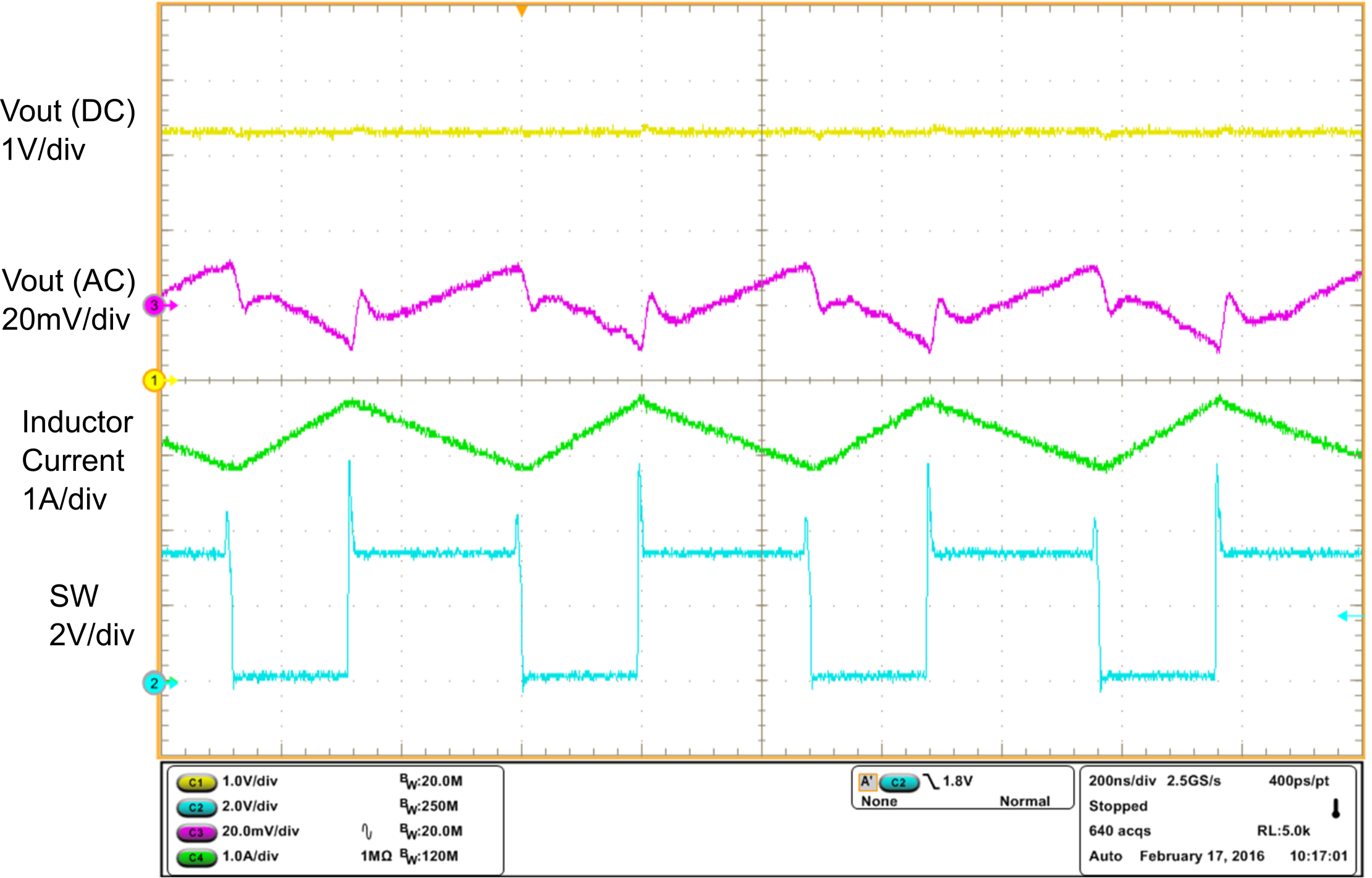
| VIN = 2.4 V, VOUT = 3.3 V, IOUT = 2 A | ||
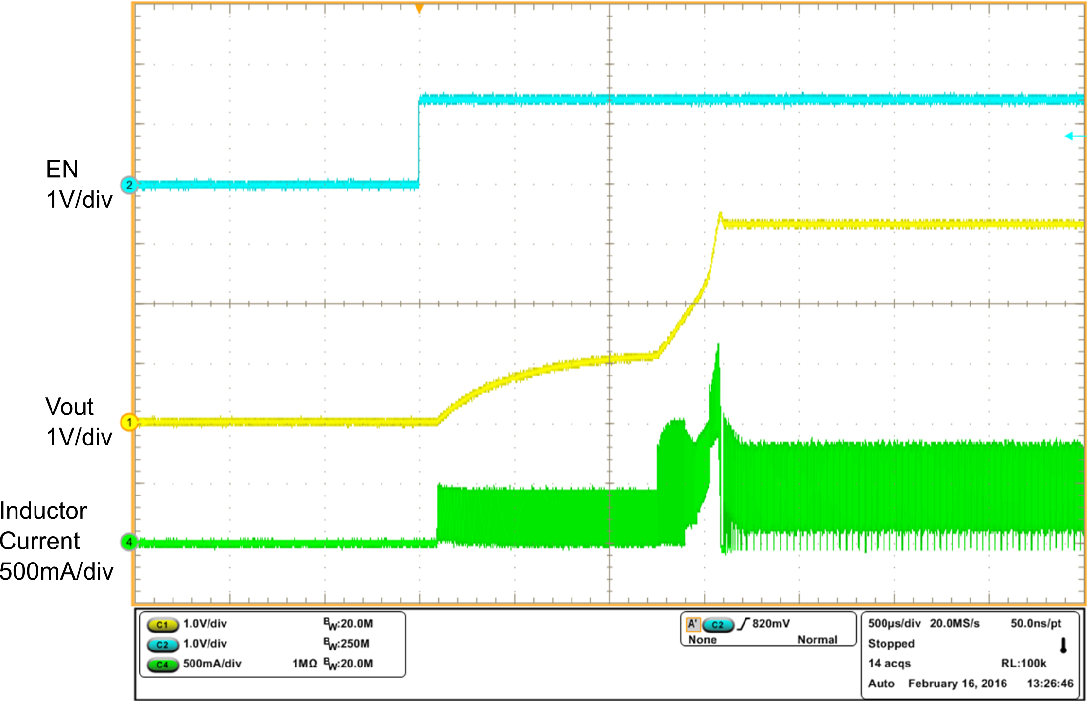
| VIN = 2.4 V, VOUT = 3.3 V, 12 Ω resistance load | ||
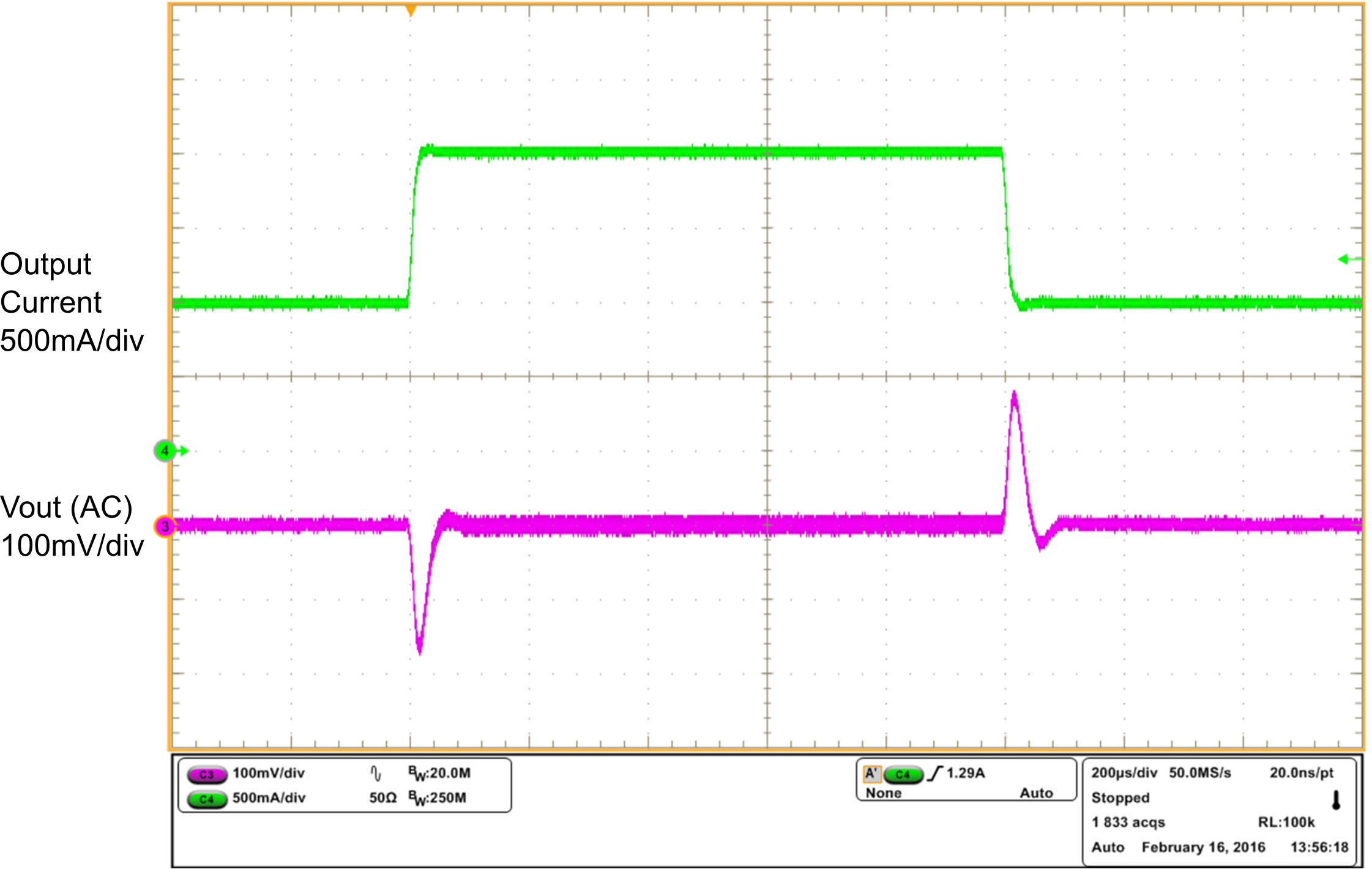
| VIN = 2.4 V, VOUT = 3.3 V, IOUT = 1 A to 2 A | ||

| VIN = 2.4 V, VOUT = 3.3 V, IOUT = 100 mA | ||
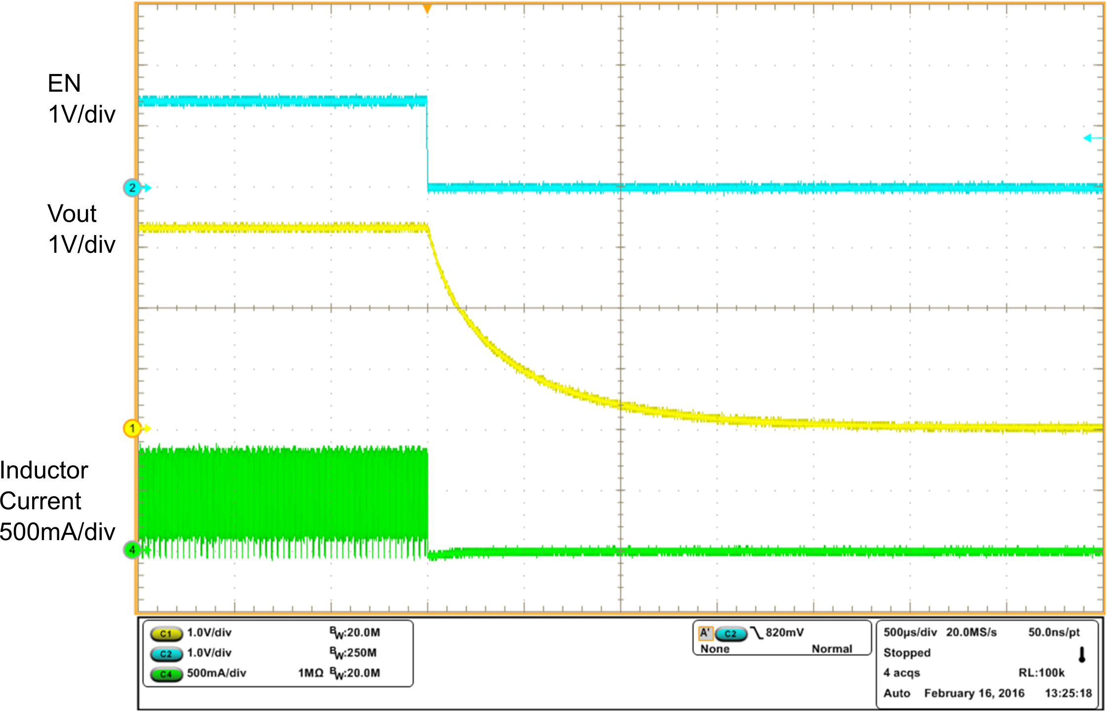
| VIN = 2.4 V, VOUT = 3.3 V, 12 Ω resistance load | ||
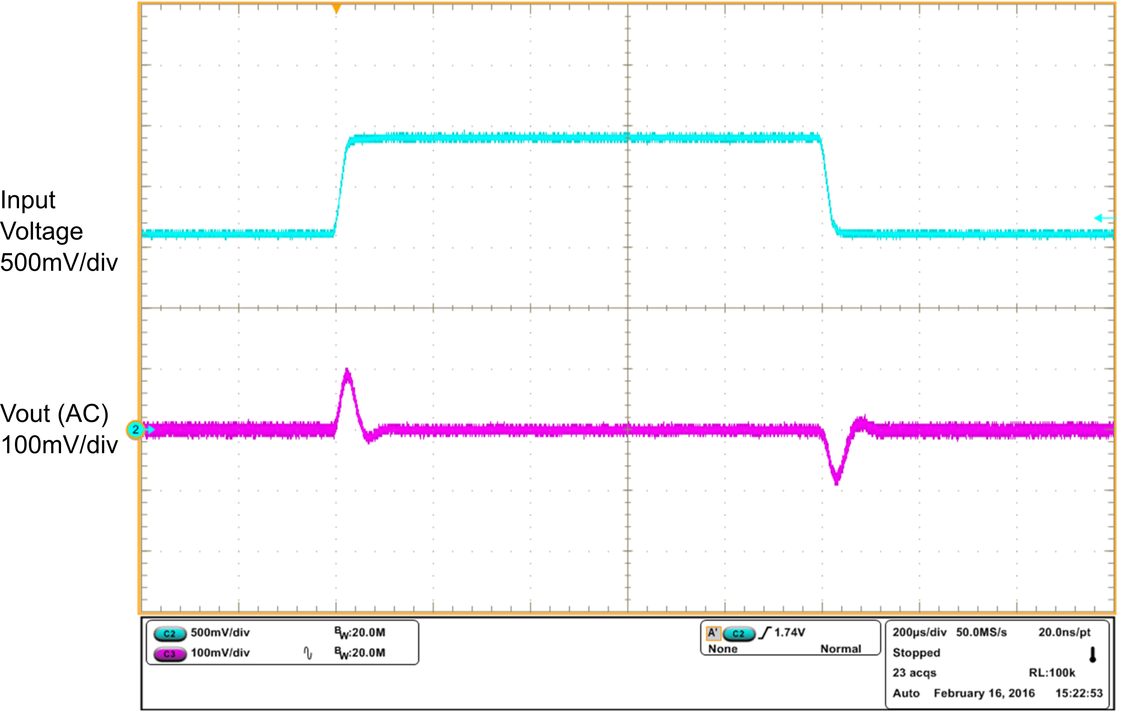
| VIN = 1.6 V to 2.4 V, VOUT = 3.3 V, IOUT = 1 A | ||