ZHCSJM5D September 2009 – April 2019 TPS61093
PRODUCTION DATA.
- 1 特性
- 2 应用
- 3 说明
- 4 修订历史记录
- 5 Pin Configuration and Functions
- 6 Specifications
- 7 Detailed Description
- 8 Application and Implementation
- 9 Power Supply Recommendations
- 10Layout
- 11器件和文档支持
- 12机械、封装和可订购信息
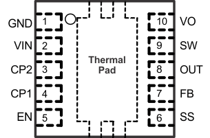
5 Pin Configuration and Functions
DSK Package
10 Pins (WSON)
Top View

Pin Functions
| PIN | I/O | DESCRIPTION | |
|---|---|---|---|
| NAME | NO. | ||
| CP1, CP2 | 3, 4 | Connect to flying capacitor for internal charge pump. | |
| EN | 5 | I | Enable pin (HIGH = enable). When the pin is pulled low for 1 ms, the IC turns off and consumes less than 1-μA current. |
| FB | 7 | I | Voltage feedback pin for output regulation, 0.5-V regulated voltage. An external resistor divider connected to this pin programs the regulated output voltage. |
| GND | 1 | – | Ground of the IC. |
| OUT | 8 | O | Isolation switch is between this pin and VO pin. Connect load to this pin for input/output isolation during IC shutdown. See Without Isolation FET for the tradeoff between isolation and efficiency. |
| SS | 6 | I | Soft start pin. A RC network connecting to the SS pin programs soft start timing. See Start-Up. |
| SW | 9 | I | Switching node of the IC where the internal PWM switch operates. |
| Thermal Pad | – | – | It should be soldered to the ground plane. If possible, use thermal via to connect to ground plane for ideal power dissipation. |
| VIN | 2 | I | IC Supply voltage input. |
| VO | 10 | O | Output of the boost converter. When the output voltage exceeds the overvoltage protection (OVP) threshold, the power switch turns off until VO drops below the overvoltage protection hysteresis. |