ZHCSKD3A November 2019 – February 2021 TPS6521815
PRODUCTION DATA
- 1 特性
- 2 应用
- 3 说明
- 4 Revision History
- 5 Description (continued)
- 6 Pin Configuration and Functions
- 7 Specifications
-
8 Detailed Description
- 8.1 Overview
- 8.2 Functional Block Diagram
- 8.3
Feature Description
- 8.3.1
Wake-Up and Power-Up and Power-Down Sequencing
- 8.3.1.1 Power-Up Sequencing
- 8.3.1.2 Power-Down Sequencing
- 8.3.1.3 Strobe 1 and Strobe 2
- 8.3.1.4 Supply Voltage Supervisor and Power-Good (PGOOD)
- 8.3.1.5 Backup Supply Power-Good (PGOOD_BU)
- 8.3.1.6 Internal LDO (INT_LDO)
- 8.3.1.7 Current Limited Load Switches
- 8.3.1.8 LDO1
- 8.3.1.9 Coin Cell Battery Voltage Acquisition
- 8.3.1.10 UVLO
- 8.3.1.11 Power-Fail Comparator
- 8.3.1.12 Battery-Backup Supply Power-Path
- 8.3.1.13 DCDC3 and DCDC4 Power-Up Default Selection
- 8.3.1.14 I/O Configuration
- 8.3.1.15 Push Button Input (PB)
- 8.3.1.16 AC_DET Input (AC_DET)
- 8.3.1.17 Interrupt Pin (INT)
- 8.3.1.18 I2C Bus Operation
- 8.3.1
Wake-Up and Power-Up and Power-Down Sequencing
- 8.4 Device Functional Modes
- 8.5 Programming
- 8.6 Register Maps
- 9 Application and Implementation
- 10Power Supply Recommendations
- 11Layout
- 12Device and Documentation Support
- 13Mechanical, Packaging, and Orderable Information
8.3.1.4 Supply Voltage Supervisor and Power-Good (PGOOD)
Power-good (PGOOD) is an open-drain output of the built-in voltage supervisor that monitors DCDC1, DCDC2, DCDC3, DCDC4, and LDO1. The output is Hi-Z when all enabled rails are in regulation and driven low when one or more rails encounter a fault which brings the output voltage outside the specified tolerance range. In a typical application PGOOD drives the reset signal of the SOC.
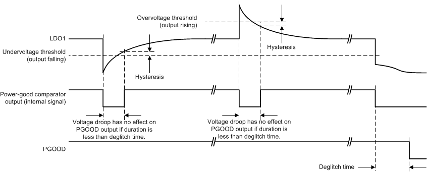
The supervisor has two modes of operation, controlled by the STRICT bit. With the STRICT bit set to 0, all enabled rails of the five regulators are monitored for undervoltage only with relaxed thresholds and deglitch times. With the STRCT bit set to 1, all enabled rails of the five regulators are monitored for undervoltage and overvoltage with tight limits and short deglitch times. #TABLE_EJN_NG4_QNB summarizes these details.
| PARAMETER | STRICT = 0b (TYP) | STRICT =1b (TYP) | |
|---|---|---|---|
| Undervoltage monitoring | Threshold (output falling) | 90% | 96.5% (DCDC1 and DCDC2) 95.5% (DCDC3, DCDC4, and LDO1) |
| Deglitch (output falling) | 1 ms | 50 µs | |
| Deglitch (output rising) | 10 µs | 10 µs | |
| Overvoltage monitoring | Threshold (output falling) | N/A | 103.5% (DCDC1 and DCDC2) 104.5% (DCDC3, DCDC4, and LDO1) |
| Deglitch (output falling) | N/A | 1 ms | |
| Deglitch (output rising) | N/A | 50 µs | |
 Figure 8-7 Definition of Undervoltage, Overvoltage Thresholds, Hysteresis, and Deglitch
Times
Figure 8-7 Definition of Undervoltage, Overvoltage Thresholds, Hysteresis, and Deglitch
TimesThe following rules apply to the PGOOD output:
- The power-up default state for THE PGOOD is low. When all rails are disabled, the PGOOD output is driven low.
- Only enabled rails are monitored. Disabled rails are ignored.
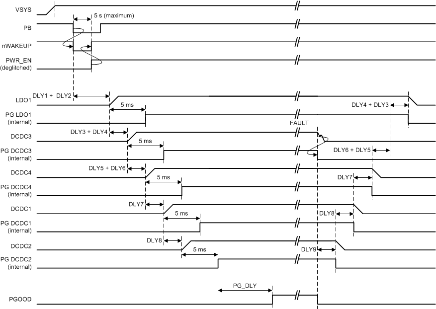
- Power-good monitoring of a particular rail starts 5 ms after the rail is enabled and is continuously monitored thereafter. This allows the rail to power-up.
- The PGOOD is delayed by PGDLY time after the sequencer is finished and the last rail is enabled.
- If an enabled rail is continuously outside the monitoring threshold for longer than the deglitch time, then the PGOOD is pulled low, and all rails are shut-down following the power-down sequence. PGDLY does not apply.
- Disabling a rail manually by resetting the DCx_EN or LDO1_EN bit has no effect on the PGOOD pin. If all rails are disabled, the PGOOD is driven low as the last rail is disabled.
- If the power-down sequencer is triggered, PGOOD is driven low.
- The PGOOD is driven low in the SUSPEND state, regardless of the number of rails that are enabled.
#SLDS2067476 shows a typical power-up sequence and PGOOD timing.
