ZHCSDM4D december   2014  – may 2023 TPS65263-Q1

PRODUCTION DATA  

  1.   1
  2. 特性
  3. 应用
  4. 说明
  5. Revision History
  6. Pin Configuration and Functions
  7. Specifications
    1. 6.1 Absolute Maximum Ratings
    2. 6.2 ESD Ratings
    3. 6.3 Recommended Operating Conditions
    4. 6.4 Thermal Information
    5. 6.5 Electrical Characteristics
    6. 6.6 Typical Characteristics
  8. Detailed Description
    1. 7.1 Overview
    2. 7.2 Functional Block Diagram
    3. 7.3 Feature Description
      1. 7.3.1  Adjusting the Output Voltage
      2. 7.3.2  Enable and Adjusting UVLO
      3. 7.3.3  Soft-Start Time
      4. 7.3.4  Power-Up Sequencing
      5. 7.3.5  V7V Low-Dropout Regulator and Bootstrap
      6. 7.3.6  Out-of-Phase Operation
      7. 7.3.7  Output Overvoltage Protection (OVP)
      8. 7.3.8  PSM
      9. 7.3.9  Slope Compensation
      10. 7.3.10 Overcurrent Protection
        1. 7.3.10.1 High-Side MOSFET Overcurrent Protection
        2. 7.3.10.2 Low-Side MOSFET Overcurrent Protection
      11. 7.3.11 Power Good
        1. 7.3.11.1 Adjustable Switching Frequency
      12. 7.3.12 Thermal Shutdown
    4. 7.4 Device Functional Modes
      1. 7.4.1 Serial Interface Description
      2. 7.4.2 I2C Update Sequence
    5. 7.5 Register Maps
      1. 7.5.1 VOUT2_SEL: Vout2 Voltage Selection Register (Address = 0x01H)
      2. 7.5.2 VOUT1_COM: Buck1 Command Register (offset = 0x03H)
      3. 7.5.3 VOUT2_COM: Buck2 Command Register (offset = 0x04H)
      4. 7.5.4 VOUT3_COM: Buck3 Command Register (offset = 0x05H)
      5. 7.5.5 SYS_STATUS: System Status Register (offset = 0x06H)
  9. Application and Implementation
    1. 8.1 Application Information
    2. 8.2 Typical Application
      1. 8.2.1 Design Requirements
      2. 8.2.2 Detailed Design Procedure
        1. 8.2.2.1 Output Inductor Selection
        2. 8.2.2.2 Output Capacitor Selection
        3. 8.2.2.3 Input Capacitor Selection
        4. 8.2.2.4 Loop Compensation
      3. 8.2.3 Application Curves
    3. 8.3 Power Supply Recommendations
    4. 8.4 Layout
      1. 8.4.1 Layout Guidelines
      2. 8.4.2 Layout Example
  10. Device and Documentation Support
    1. 9.1 接收文档更新通知
    2. 9.2 支持资源
    3. 9.3 Trademarks
    4. 9.4 静电放电警告
    5. 9.5 术语表
  11. 10Mechanical, Packaging, and Orderable Information

封装选项

机械数据 (封装 | 引脚)
散热焊盘机械数据 (封装 | 引脚)
订购信息

Application Curves

GUID-B8296B11-8D4F-485E-9A27-992289D1381A-low.png
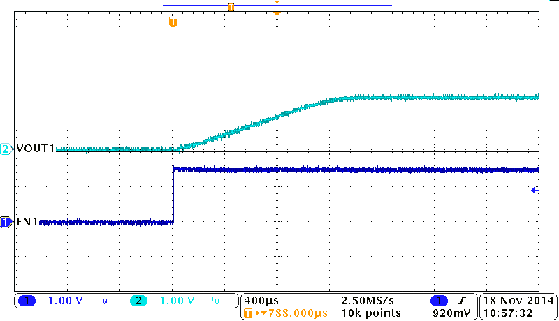
Iout = 3 A
Figure 8-3 BUCK1, Soft Start
GUID-734A4EF8-F8BA-4DA5-9F8C-2972F2179567-low.png
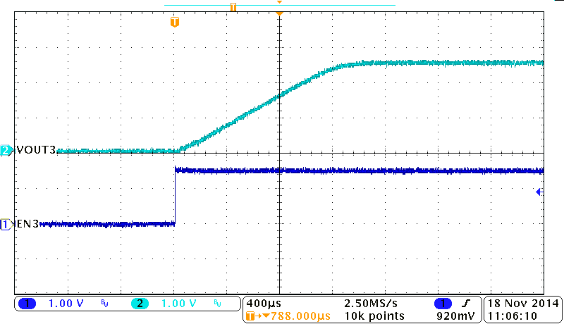
Iout = 2 A
Figure 8-5 BUCK3, Soft Start
GUID-30B1AEA5-26DE-4262-91CD-25475BFC05F2-low.png
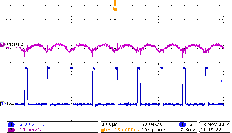
Iout = 2 A
Figure 8-7 BUCK2, Output Voltage Ripple
GUID-AA4408B7-3A30-4FEC-9145-5D31AD5F2335-low.png
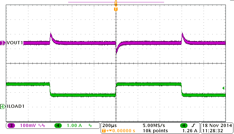
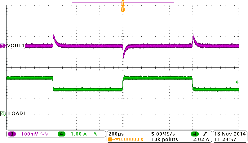
0.75 to 1.5 A SR = 0.25 A/µs
Figure 8-9 BUCK1, Load Transient
GUID-3398EA97-76E2-4F8B-B7EB-1C0098500365-low.png
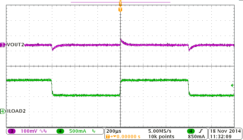
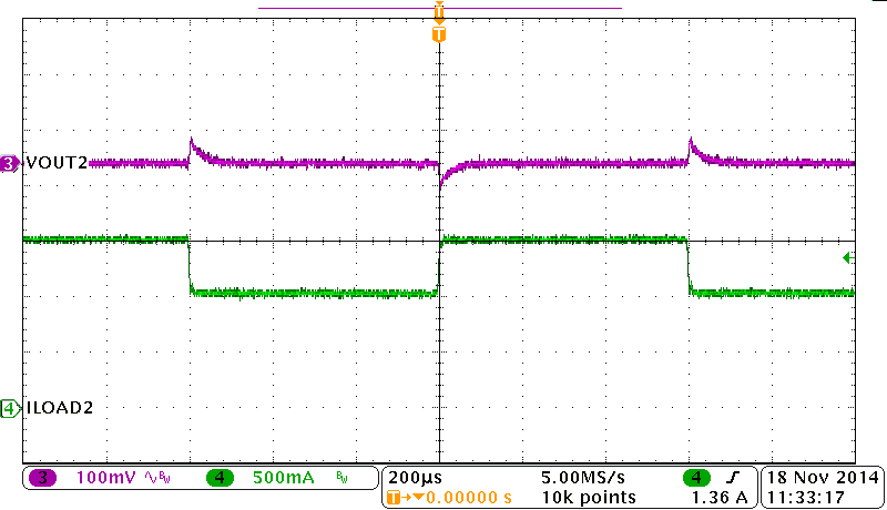
0.5 to 1.0 A SR = 0.25 A/µs
Figure 8-11 BUCK2, Load Transient
GUID-4A41899C-8373-43F2-965C-E7A508CB3307-low.png
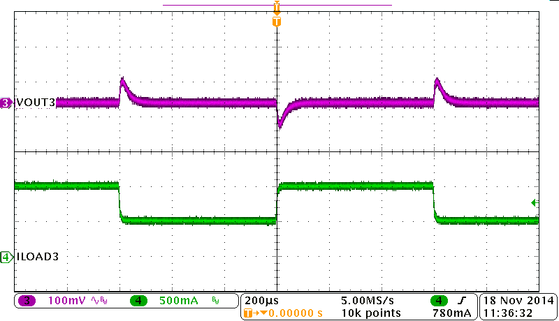
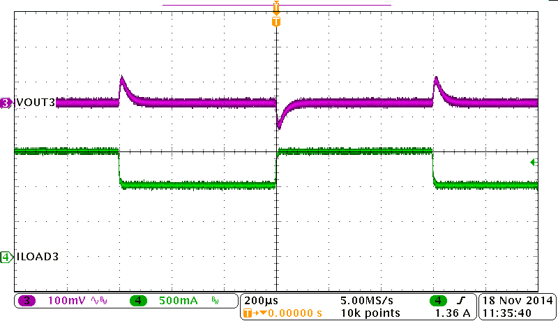
0.5 to 1.0 A SR = 0.25 A/µs
Figure 8-13 BUCK3, Load Transient
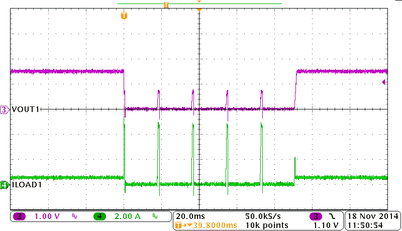
GUID-13BF0D9C-2CE7-4C40-A740-906BCB816E0E-low.pngFigure 8-15 BUCK1, Hiccup and Recovery
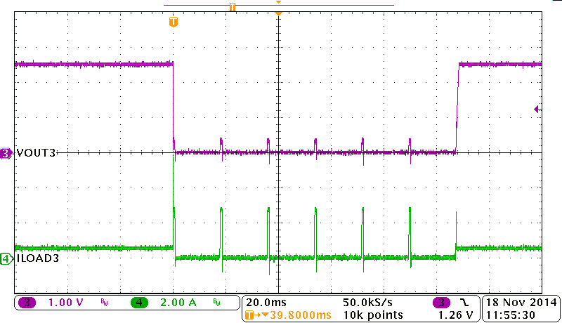
GUID-9D8D87F2-713C-4698-AA13-5425A4C840B6-low.pngFigure 8-17 BUCK3, Hiccup and Recovery
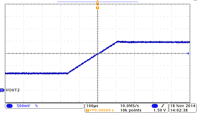
GUID-AA470FF7-CF7E-49CC-8F44-DADCDA9ABE8C-low.pngFigure 8-19 VID2 from 00 to 7F, SR = 10 mV/Cycle
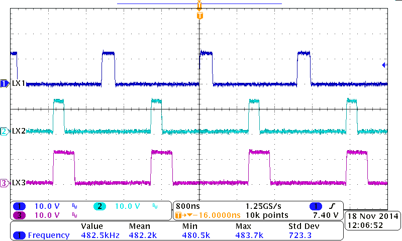
GUID-F0C1E99C-D9B6-472F-99FB-E6703687C0D1-low.pngFigure 8-21 180° Out-of-Phase
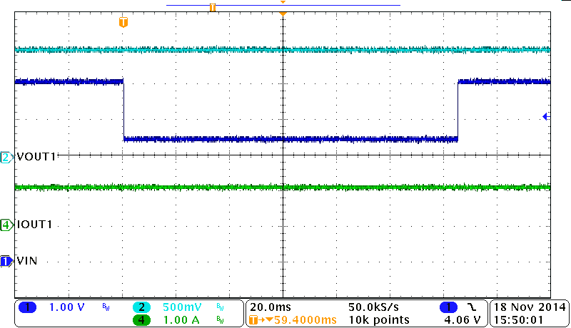
GUID-805F79D5-75C0-4F2B-ACF5-E92E651007FE-low.pngFigure 8-23 Operation at VIN Drop to 2.5 V
GUID-9C00783E-8C0B-43B5-90F9-026FAF43F209-low.png
Iout = 2 A
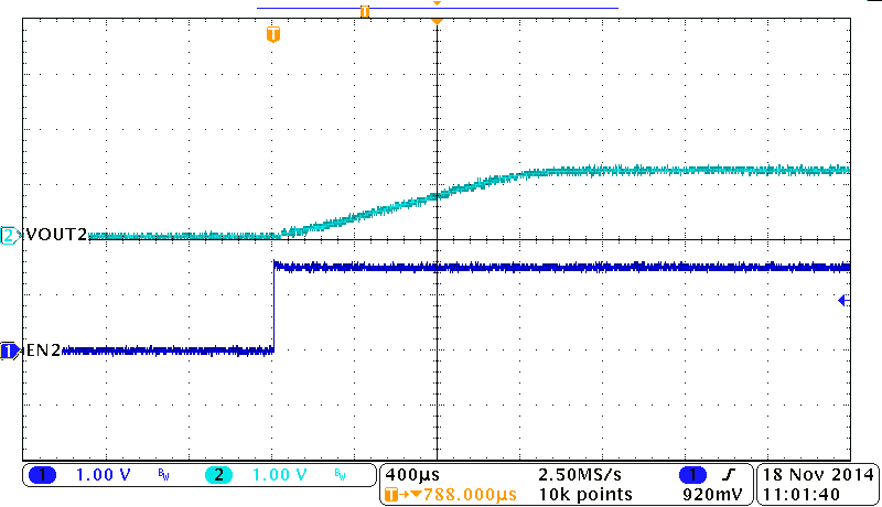
Figure 8-4 BUCK2, Soft Start
GUID-4DDF8EE6-F870-46C6-B917-8368C0173444-low.png
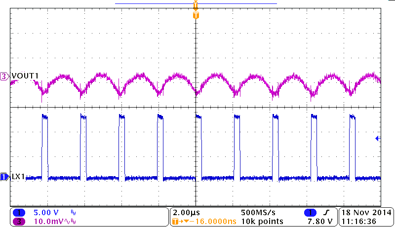
Iout = 3 A
Figure 8-6 BUCK1, Output Voltage Ripple
GUID-46176A4F-5FFA-43A3-B27A-6538DD1D8258-low.png
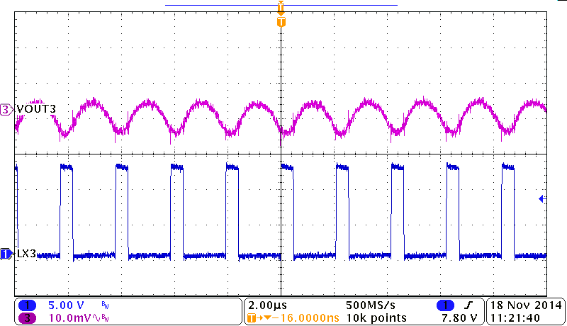
Iout = 2 A
Figure 8-8 BUCK3, Output Voltage Ripple
GUID-25413340-CFF5-4846-827B-71A6BC002210-low.png
1.5 to 2.25 A SR = 0.25 A/µs
Figure 8-10 BUCK1, Load Transient
GUID-FE5E3ABA-B856-46B5-874D-6670BC73F605-low.png
1.0 to 1.5 A SR = 0.25 A/µs
Figure 8-12 BUCK2, Load Transient
GUID-D0570889-2A90-48BF-B4C4-2652C2720330-low.png
1.0 to 1.5 A SR = 0.25 A/µs
Figure 8-14 BUCK3, Load Transient
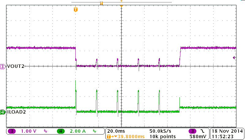
GUID-3864043B-A085-4215-8D40-FDED3569ED5B-low.pngFigure 8-16 BUCK2, Hiccup and Recovery
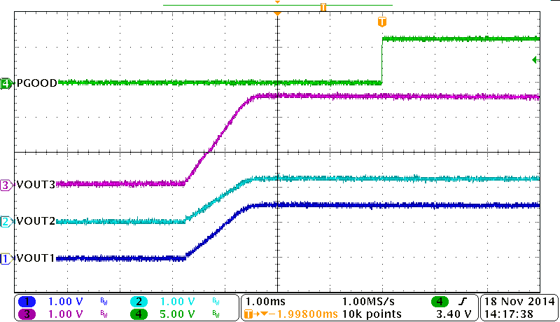
GUID-209EE46A-4E55-432C-9532-310237D9264E-low.pngFigure 8-18 PGOOD
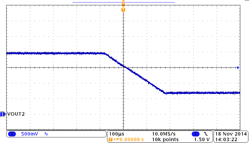
GUID-4FC23E39-2DD4-4728-8632-4960273C65DC-low.pngFigure 8-20 VID2 from 7F to 00, SR = 10 mV/Cycle
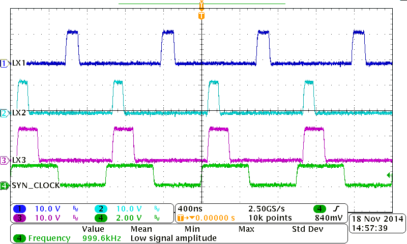
GUID-C4BFDE04-0145-4765-B138-B101818F1D22-low.pngFigure 8-22 Synchronization with External Clock
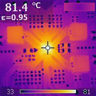
GUID-6469BBD7-B33D-46A5-A916-9BFBA2FCD0BC-low.png
VIN = 12 V, VOUT1 = 1.5 V/3 A, VOUT2 = 1.2 V/2 A,
VOUT3 = 2.5 V/2 A,
TA = 26.8°C EVM condition 4 layers, 75 mm × 75 mm
Figure 8-24 Thermal Signature of TPS65263-Q1EVM Operating