SBVS054J November 2004 – April 2015 TPS730
PRODUCTION DATA.
- 1 Features
- 2 Applications
- 3 Description
- 4 Revision History
- 5 Pin Configuration and Functions
- 6 Specifications
- 7 Detailed Description
- 8 Application and Implementation
- 9 Power Supply Recommendations
- 10Layout
- 11Device and Documentation Support
- 12Mechanical, Packaging, and Orderable Information
10 Layout
10.1 Layout Guidelines
Layout is a critical part of good power-supply design. There are several signal paths that conduct fast-changing currents or voltages that can interact with stray inductance or parasitic capacitance to generate noise or degrade the power-supply performance. To help eliminate these problems, the IN pin should be bypassed to ground with a low ESR ceramic bypass capacitor with an X5R or X7R dielectric.
Equivalent series inductance (ESL) and equivalent series resistance (ESR) must be minimized to maximize performance and ensure stability. Every capacitor (CIN, COUT, CNR/SS, CFF) must be placed as close as possible to the device and on the same side of the PCB as the regulator itself.
Do not place any of the capacitors on the opposite side of the PCB from where the regulator is installed. The use of vias and long traces is strongly discouraged because these circuits may impact system performance negatively, and even cause instability.
10.1.1 Board Layout Recommendations to Improve PSRR and Noise Performance
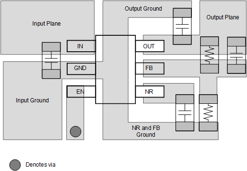
To improve AC measurements like PSRR, output noise, and transient response, TI recommends designing the board with separate ground planes for VIN and VOUT, with each ground plane connected only at the GND pin of the device. In addition, the ground connection for the bypass capacitor should connect directly to the GND pin of the device.
10.2 Layout Example
 Figure 23. Layout Example (DBV Package)
10.3 Thermal Considerations
Thermal protection disables the output when the junction temperature rises to approximately 165°C, allowing the device to cool. When the junction temperature cools to approximately 140°C, the output circuitry is again enabled. Depending on power dissipation, thermal resistance, and ambient temperature, the thermal protection circuit may cycle on and off. This cycling limits regulator dissipation, protecting the device from damage as a result of overheating.
Any tendency to activate the thermal protection circuit indicates excessive power dissipation or an inadequate heatsink. For reliable operation, junction temperature must be limited to 125°C maximum. To estimate the margin of safety in a complete design (including heatsink), increase the ambient temperature until the thermal protection is triggered; use worst-case loads and signal conditions.
The TPS730 internal protection circuitry is designed to protect against overload conditions. This circuitry is not intended to replace proper heatsinking. Continuously running the TPS730 into thermal shutdown degrades device reliability.
10.4 Power Dissipation
Specified regulator operation is assured to a junction temperature of +125°C; the maximum junction temperature should be restricted to +125°C under normal operating conditions. This restriction limits the power dissipation the regulator can handle in any given application. To ensure the junction temperature is within acceptable limits, calculate the maximum allowable dissipation, PD(max), and the actual dissipation, PD, which must be less than or equal to PD(max).
The maximum power dissipation limit is determined using Equation 4:

where
- TJmax is the maximum allowable junction temperature.
- RθJA is the thermal resistance junction-to-ambient for the package (see the Thermal Information table).
- TA is the ambient temperature.
The regulator dissipation is calculated using Equation 5:

Power dissipation resulting from quiescent current is negligible. Excessive power dissipation triggers the thermal protection circuit.
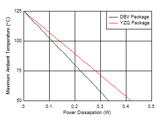
Figure 24 shows the maximum ambient temperature versus the power dissipation of the TPS730. This figure assumes the device is soldered on a JEDEC standard, high-K layout with no airflow over the board. Actual board thermal impedances vary widely. If the application requires high power dissipation, having a thorough understanding of the board temperature and thermal impedances is helpful to ensure the TPS730 does not operate above a junction temperature of 125°C.
 Figure 24. Maximum Ambient Temperature vs Power Dissipation
Estimating the junction temperature can be done by using the thermal metrics ΨJT and ΨJB, shown in the Thermal Information table. These metrics are a more accurate representation of the heat transfer characteristics of the die and the package than RθJA. The junction temperature can be estimated with Equation 6.

where
- PD is the power dissipation shown by Equation 5,
- TT is the temperature at the center-top of the IC package,
- TB is the PCB temperature measured 1 mm away from the IC package on the PCB surface.
NOTE
Both TT and TB can be measured on actual application boards using a thermo‐gun (an infrared thermometer).
For more information about measuring TT and TB, see the application note Using New Thermal Metrics (SBVA025), available for download at www.ti.com.