ZHCSAL3R December 2005 – April 2017 TPS74401
PRODUCTION DATA.
- 1 特性
- 2 应用
- 3 说明
- 4 修订历史记录
- 5 Pin Configuration and Functions
- 6 Specifications
- 7 Detailed Description
- 8 Application and Implementation
- 9 Power Supply Recommendations
- 10Layout
- 11器件和文档支持
- 12机械、封装和可订购信息
封装选项
机械数据 (封装 | 引脚)
散热焊盘机械数据 (封装 | 引脚)
订购信息
10 Layout
10.1 Layout Guidelines
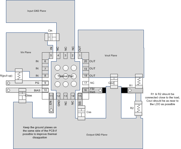
An optimal layout can greatly improve transient performance, PSRR, and noise. To minimize the voltage droop on the input of the device during load transients, connect the capacitance on IN and BIAS as close as possible to the device. This capacitance also minimizes the effects of parasitic inductance and resistance of the input source and can therefore improve stability. To achieve optimal transient performance and accuracy, connect the top side of R1 in Figure 27 as close as possible to the load. This connection minimizes the voltage droop on BIAS during transient conditions and can improve the turn-on response.
10.3 Power Dissipation
Knowing the device power dissipation and proper sizing of the thermal plane that is connected to the tab or pad is critical to avoiding thermal shutdown and ensuring reliable operation.
Power dissipation of the device depends on input voltage and load conditions, and can be calculated using Equation 5:

Power dissipation can be minimized and greater efficiency can be achieved by using the lowest possible input voltage necessary to achieve the required output voltage regulation.
On the VQFN (RGW, RGR) packages, the primary conduction path for heat is through the exposed pad to the PCB. The pad can be connected to ground or left floating; however, the pad must be attached to an appropriate amount of copper PCB area to ensure the device does not overheat. On the DDPAK (KTW) package, the primary conduction path for heat is through the tab to the PCB. Connect that tab to ground. The maximum junction-to-ambient thermal resistance depends on the maximum ambient temperature, maximum device junction temperature, and power dissipation of the device and can be estimated using Equation 6:

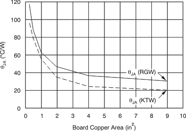
Knowing the maximum RθJA, the minimum amount of PCB copper area needed for appropriate heatsinking can be estimated using Figure 41.

NOTE:
θJA value at board size of 9 in2 (that is, 3 in × 3 in) is a JEDEC standard.Figure 41 shows the variation of θJA as a function of ground plane copper area in the board. Figure 41 is intended only as a guideline to demonstrate the affects of heat spreading in the ground plane; do not use Figure 41 to estimate actual thermal performance in real application environments.
NOTE
When the device is mounted on an application PCB, TI strongly recommends using ΨJT and ΨJB, as explained in the section.
10.4 Thermal Considerations
A better method of estimating the thermal measure comes from using the thermal metrics ΨJT and ΨJB, as shown in Thermal Information . These metrics are a more accurate representation of the heat transfer characteristics of the die and the package than RθJA. The junction temperature can be estimated with the corresponding formulas given in Equation 7.

where
- PD is the power dissipation shown by Equation 5,
- TT is the temperature at the center-top of the IC package, and
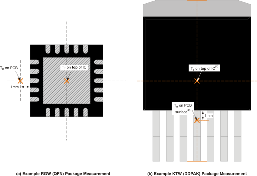
- TB is the PCB temperature measured 1 mm away from the IC package on the PCB surface (see Figure 42).
NOTE
Both TT and TB can be measured on actual application boards using a thermo‐gun (an infrared thermometer).
For more information about measuring TT and TB, see the application note Using New Thermal Metrics (SBVA025), available for download at www.ti.com.

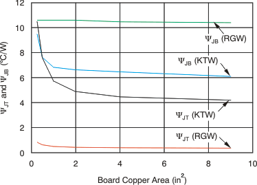
Compared with θJA, the thermal metrics ΨJT and ΨJB are less independent of board size, but do have a small dependency on board size and layout. Figure 43 shows characteristic performance of ΨJT and ΨJB versus board size.
Referring to Figure 43, the RGW package thermal performance has negligible dependency on board size. The KTW package, however, does have a measurable dependency on board size. This dependency exists because the package shape is not point symmetric to an IC center. In the KTW package, for example (see Figure 42), silicon is not beneath the measuring point of TT which is the center of the X and Y dimension, so that ΨJT has a dependency. Also, because of that non-point symmetry, device heat distribution on the PCB is not point symmetric either, so that ΨJB has a greater dependency on board size and layout.
 Figure 43. ΨJT and ΨJB versus Board Size
For a more detailed discussion of why TI does not recommend using θJC(top) to determine thermal characteristics, refer to the application note Using New Thermal Metrics (SBVA025), available for download at www.ti.com. Also, refer to the application note IC Package Thermal Metrics (SPRA953) (also available on the TI website) for further information.
