ZHCSAL3R December 2005 – April 2017 TPS74401
PRODUCTION DATA.
- 1 特性
- 2 应用
- 3 说明
- 4 修订历史记录
- 5 Pin Configuration and Functions
- 6 Specifications
- 7 Detailed Description
- 8 Application and Implementation
- 9 Power Supply Recommendations
- 10Layout
- 11器件和文档支持
- 12机械、封装和可订购信息
封装选项
机械数据 (封装 | 引脚)
散热焊盘机械数据 (封装 | 引脚)
订购信息
6 Specifications
6.1 Absolute Maximum Ratings
over operating free-air temperature range (unless otherwise noted)(1)| MIN | MAX | UNIT | ||
|---|---|---|---|---|
| VIN, VBIAS | Input voltage | –0.3 | 6 | V |
| VEN | Enable voltage | –0.3 | 6 | V |
| VPG | Power-good voltage | –0.3 | 6 | V |
| IPG | PG sink current | 0 | 1.5 | mA |
| VSS | SS pin voltage | –0.3 | 6 | V |
| VFB | Feedback pin voltage | –0.3 | 6 | V |
| VOUT | Output voltage | –0.3 | VIN + 0.3 | V |
| IOUT | Maximum output current | Internally limited | ||
| Output short-circuit duration | Indefinite | |||
| PDISS | Continuous total power dissipation | See Thermal Information | ||
| TJ | Operating junction temperature | –40 | 150 | °C |
| Tstg | Storage temperature | –55 | 150 | °C |
(1) Stresses beyond those listed under Absolute Maximum Ratings may cause permanent damage to the device. These are stress ratings only, which do not imply functional operation of the device at these or any other conditions beyond those indicated under Recommended Operating Conditions. Exposure to absolute-maximum-rated conditions for extended periods may affect device reliability.
6.2 ESD Ratings
| VALUE | UNIT | |||
|---|---|---|---|---|
| V(ESD) | Electrostatic discharge | Human body model (HBM), per ANSI/ESDA/JEDEC JS-001(1) | ±2000 | V |
| Charged device model (CDM), per JEDEC specification JESD22-C101(2) | ±500 | |||
(1) JEDEC document JEP155 states that 500-V HBM allows safe manufacturing with a standard ESD control process.
(2) JEDEC document JEP157 states that 250-V CDM allows safe manufacturing with a standard ESD control process.
6.3 Recommended Operating Conditions
over operating free-air temperature range (unless otherwise noted)| MIN | NOM | MAX | UNIT | ||
|---|---|---|---|---|---|
| VIN | Input supply voltage range | 1.1 | 5.5 | V | |
| VEN | Enable supply voltage range | 0 | 5.5 | V | |
| VBIAS(1) | BIAS supply voltage range | VOUT + VDO (VBIAS) | 5.5 | V | |
| IOUT | Output current | 0 | 3 | A | |
| COUT | Output capacitor | 0 | µF | ||
| CIN(2) | Input capacitor | 1 | µF | ||
| CBIAS | Bias capacitor | 1 | µF | ||
| TJ | Operating junction temperature | –40 | 125 | °C | |
(2) If VIN and VBIAS are connected to the same supply, the recommended minimum capacitor for the supply is 4.7 µF.
6.4 Thermal Information
| THERMAL METRIC(1)(2) | TPS74401(3) | UNIT | |||
|---|---|---|---|---|---|
| RGW (VQFN) |
RGR (VQFN) |
KTW (DDPAK) |
|||
| 20 PINS | 20 PINS | 7 PINS | |||
| RθJA | Junction-to-ambient thermal resistance | 35.4 | 39.1 | 26.6 | °C/W |
| RθJC(top) | Junction-to-case (top) thermal resistance | 32.4 | 29.3 | 41.7 | °C/W |
| RθJB | Junction-to-board thermal resistance | 14.7 | 10.2 | 12.5 | °C/W |
| ψJT | Junction-to-top characterization parameter | 0.4 | 0.4 | 4.0 | °C/W |
| ψJB | Junction-to-board characterization parameter | 14.8 | 10.1 | 7.3 | °C/W |
| RθJC(bot) | Junction-to-case (bottom) thermal resistance | 3.9 | 2.0 | 0.3 | °C/W |
(1) For more information about traditional and new thermal metrics, see the Semiconductor and IC Package Thermal Metrics application report.
(2) For thermal estimates of this device based on PCB copper area, see the TI PCB Thermal Calculator.
(3) Thermal data for the RGW, RGR, and KTW packages are derived by thermal simulations based on JEDEC-standard methodology as specified in the JESD51 series. The following assumptions are used in the simulations:
- i. RGW and RGR: The exposed pad is connected to the PCB ground layer through a 4x4 thermal via array.
- ii. KTW: The exposed pad is connected to the PCB ground layer through a 6x6 thermal via array. - Each of top and bottom copper layers has a dedicated pattern for 20% copper coverage.
- These data were generated with only a single device at the center of a JEDEC high-K (2s2p) board with 3in × 3in copper area. To understand the effects of the copper area on thermal performance, refer to the Thermal Considerations section.
6.5 Electrical Characteristics
At VEN = 1.1 V, VIN = VOUT + 0.3 V, CIN = CBIAS = 0.1 μF, COUT = 10 μF, IOUT = 50 mA, VBIAS = 5.0 V, and TJ = –40°C to 125°C, unless otherwise noted. Typical values are at TJ = 25°C.| PARAMETER | TEST CONDITIONS | MIN | TYP | MAX | UNIT | |
|---|---|---|---|---|---|---|
| VIN | Input voltage range | VOUT + VDO | 5.5 | V | ||
| VBIAS | Bias pin voltage range | 2.375 | 5.25 | V | ||
| VREF | Internal reference | TJ = 25°C | 0.796 | 0.8 | 0.804 | V |
| VOUT | Output voltage range | VIN = 5 V, IOUT = 1.5 A, VBIAS = 5 V | VREF | 3.6 | V | |
| Accuracy | 2.97 V ≤ VBIAS ≤ 5.25 V, VOUT + 1.62 V ≤ VBIAS, 50 mA ≤ IOUT ≤ 3.0 A(1) |
–1% | ±0.2% | 1% | ||
| VOUT + VDO BIAS ≤ VBIAS ≤ 5.25 V, 100 mA ≤ IOUT ≤ I VDO BIAS , VQFN(2) |
–1% | ±0.2% | 1% | |||
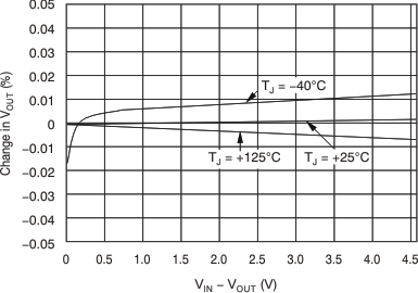
| ΔVOUT(ΔVIN) | Line regulation | VOUT(nom) + 0.3 ≤ VIN ≤ 5.5 V, VQFN | 0.0005 | 0.05 | %/V | |
| VOUT(nom) + 0.3 ≤ VIN ≤ 5.5 V, DDPAK | 0.0005 | 0.06 | ||||
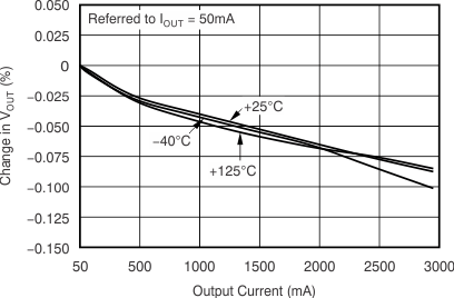
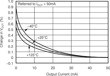
| ΔVOUT(ΔIOUT) | Load regulation | 0 mA ≤ IOUT ≤ 50 mA | 0.013 | %/mA | ||
| 50 mA ≤ IOUT ≤ 3.0 A | 0.03 | %/A | ||||
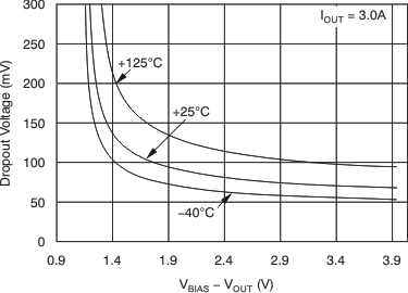
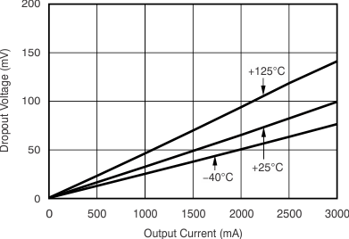
| VDO | VIN dropout voltage(3) | IOUT = 3.0 A, VBIAS – VOUT(nom) ≥ 1.62 V, VQFN | 115 | 195 | mV | |
| IOUT = 3.0 A, VBIAS – VOUT(nom) ≥ 1.62 V, DDPAK | 120 | 240 | ||||
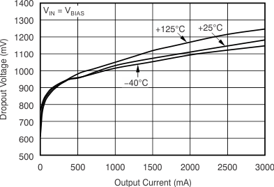
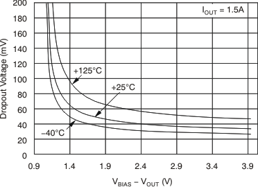
| VBIAS dropout voltage(3) | IOUT = 3.0 A, VIN = VBIAS | 1.62 | V | |||
| IOUT = 3.0 A | 1.62 | |||||
| IOUT = 1.0 A | 1.35 | |||||
| IOUT = 500 mA | 1.27 | |||||
| IOUT = 100 mA | 1.16 | |||||
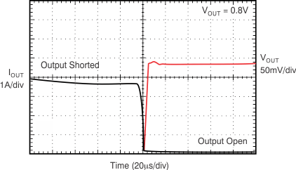
| ICL | Current limit | VOUT = 80% × VOUT(nom), VQFN | 3.8 | 6.0 | A | |
| VOUT = 80% × VOUT(nom), DDPAK | 3.5 | 6.0 | ||||
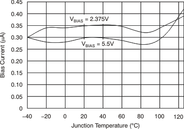
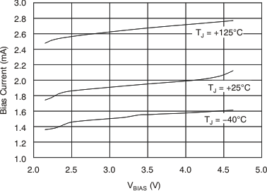
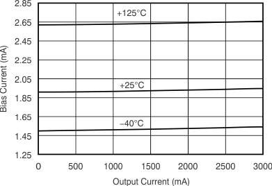
| IBIAS | Bias pin current | IOUT = 0 mA to 3.0 A | 2 | 4 | mA | |
| ISHDN | Shutdown supply current (VIN) | VEN ≤ 0.4 V | 1 | 100 | μA | |
| IFB | Feedback pin current(4) | IOUT = 50 mA to 3.0 A | –250 | 95 | 250 | nA |
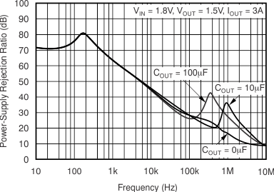
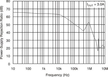
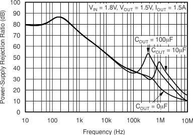
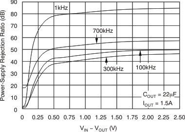
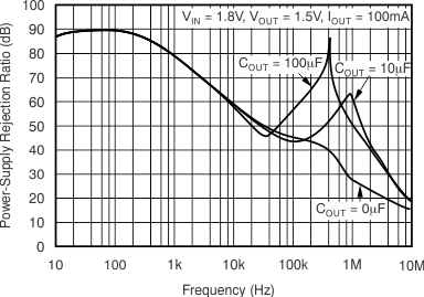
| PSRR(5) | Power-supply rejection (VIN to VOUT) |
1 kHz, IOUT = 1.5 A, VIN = 1.8 V, VOUT = 1.5 V | 73 | dB | ||
| 800 kHz, IOUT = 1.5 A, VIN = 1.8 V, VOUT = 1.5 V | 42 | |||||
| Power-supply rejection (VBIAS to VOUT) |
1 kHz, IOUT = 1.5 A, VIN = 1.8 V, VOUT = 1.5 V | 62 | dB | |||
| 800 kHz, IOUT = 1.5 A, VIN = 1.8 V, VOUT = 1.5 V | 50 | |||||
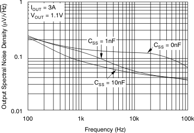
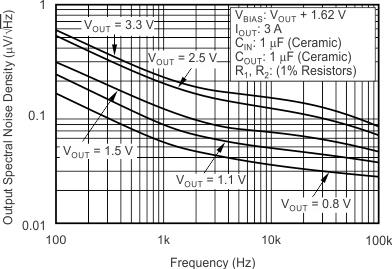
| Vn | Output noise voltage | 100 Hz to 100 kHz, IOUT = 1.5 A, CSS = 0.001 µF | 16 × VOUT | µVRMS | ||
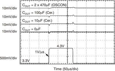
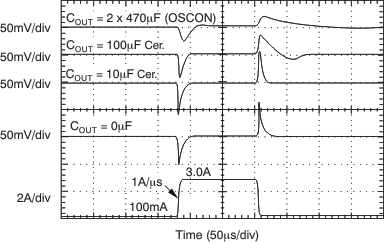
| VTRAN | %VOUT droop during load transient | IOUT = 100 mA to 3.0 A at 1 A/µs, COUT = 0 µF | 4 | %VOUT | ||
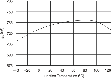
| ISS | Soft-start charging current | VSS = 0.4 V | 0.5 | 0.73 | 1 | μA |
| VEN(high) | Enable input high level | 1.1 | 5.5 | V | ||
| VEN(low) | Enable input low level | 0 | 0.4 | V | ||
| VEN(hys) | Enable pin hysteresis | 50 | mV | |||
| IEN | Enable pin current | VEN = 5 V | 0.1 | 1 | μA | |
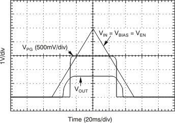
| VIT | PG trip threshold | VOUT decreasing | 86.5 | 90 | 93.5 | %VOUT |
| VHYS | PG trip hysteresis | 3 | %VOUT | |||
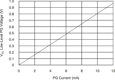
| VPG(low) | PG output low voltage | IPG = 1 mA (sinking), VOUT < VIT | 0.3 | V | ||
| IPG(lkg) | PG leakage current | VPG = 5.25 V, VOUT > VIT | 0.03 | 1 | μA | |
| TJ | Operating junction temperature | –40 | 125 | °C | ||
| TSD | Thermal shutdown temperature | Shutdown, temperature increasing | 155 | °C | ||
| Reset, temperature decreasing | 140 | |||||
(2) VOUT is set to 1.5 V to avoid minimum VBIAS restrictions.
(3) Dropout is defined as the voltage from the input to VOUT when VOUT is 2% below nominal.
(4) IFB current flow is out of the device.
6.6 Timing Requirements
At VEN = 1.1 V, VIN = VOUT + 0.3 V, CIN = CBIAS = 0.1 μF, COUT = 10 μF, IOUT = 50 mA, VBIAS = 5.0 V, and TJ = –40°C to 125°C, unless otherwise noted. Typical values are at TJ = 25°C.| MIN | NOM | MAX | UNIT | ||
|---|---|---|---|---|---|
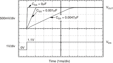
| tSTR | Minimum startup time (IOUT = 1.5 A, CSS = open) | 100 | μs | ||
| VEN(dg) | Enable pin de-glitch time | 20 | μs | ||
6.7 Typical Characteristics
At TJ = 25°C, VOUT = 1.5 V, VIN = VOUT(nom) + 0.3 V, VBIAS = 3.3 V, IOUT = 50 mA, CIN = 1 μF, CBIAS = 1 μF, CSS = 0.01 μF, and COUT = 10 μF, unless otherwise noted.