ZHCSSM4E August   1999  – March 2024 TPS766

PRODUCTION DATA  

  1.   1
  2. 特性
  3. 应用
  4. 说明
  5. Pin Configuration and Functions
  6. Specifications
    1. 5.1 Absolute Maximum Ratings
    2. 5.2 ESD Ratings
    3. 5.3 Recommended Operating Conditions
    4. 5.4 Thermal Information (Legacy Chip)
    5. 5.5 Thermal Information (New Chip)
    6. 5.6 Electrical Characteristics
    7. 5.7 Timing Diagram
    8. 5.8 Typical Characteristics
    9. 5.9 Typical Characteristics: Supported ESR Range
  7. Detailed Description
    1. 6.1 Overview
    2. 6.2 Functional Block Diagrams
    3. 6.3 Feature Description
      1. 6.3.1 Output Enable
      2. 6.3.2 Dropout Voltage
      3. 6.3.3 Current Limit
      4. 6.3.4 Undervoltage Lockout (UVLO)
      5. 6.3.5 Power-Good Function
      6. 6.3.6 Output Pulldown
      7. 6.3.7 Thermal Shutdown
    4. 6.4 Device Functional Modes
      1. 6.4.1 Device Functional Mode Comparison
      2. 6.4.2 Normal Operation
      3. 6.4.3 Dropout Operation
      4. 6.4.4 Disabled
  8. Application and Implementation
    1. 7.1 Application Information
    2. 7.2 Typical Application
      1. 7.2.1 Design Requirements
      2. 7.2.2 Detailed Design Procedure
        1. 7.2.2.1 Adjustable Device Feedback Resistors
        2. 7.2.2.2 Recommended Capacitor Types
        3. 7.2.2.3 Input and Output Capacitor Requirements
        4. 7.2.2.4 Reverse Current
        5. 7.2.2.5 Feed-Forward Capacitor (CFF)
        6. 7.2.2.6 Power Dissipation (PD)
        7. 7.2.2.7 Estimating Junction Temperature
      3. 7.2.3 Application Curves
    3. 7.3 Power Supply Recommendations
    4. 7.4 Layout
      1. 7.4.1 Layout Guidelines
      2. 7.4.2 Layout Example
  9. Device and Documentation Support
    1. 8.1 Documentation Support
      1. 8.1.1 Device Nomenclature
    2. 8.2 接收文档更新通知
    3. 8.3 支持资源
    4. 8.4 Trademarks
    5. 8.5 静电放电警告
    6. 8.6 术语表
  10. Revision History
  11. 10Mechanical, Packaging, and Orderable Information

封装选项

请参考 PDF 数据表获取器件具体的封装图。

机械数据 (封装 | 引脚)
  • D|8
散热焊盘机械数据 (封装 | 引脚)
订购信息

Reverse Current

Excessive reverse current potentially damages this device. Reverse current flows through the intrinsic body diode of the pass transistor instead of the normal conducting channel. At high magnitudes, this current flow degrades the long-term reliability of the device.

Conditions where reverse current occur are outlined in this section, all of which potentially exceed the absolute maximum rating of VOUT ≤ VIN + 0.3V.

  • If the device has a large COUT and the input supply collapses with little or no load current
  • The output is biased when the input supply is not established
  • The output is biased above the input supply

If reverse current flow is expected in the application, external protection is recommended to protect the device. Reverse current is not limited in the device, so external limiting is required if extended reverse voltage operation is anticipated.

Figure 7-3 shows one approach for protecting the device.
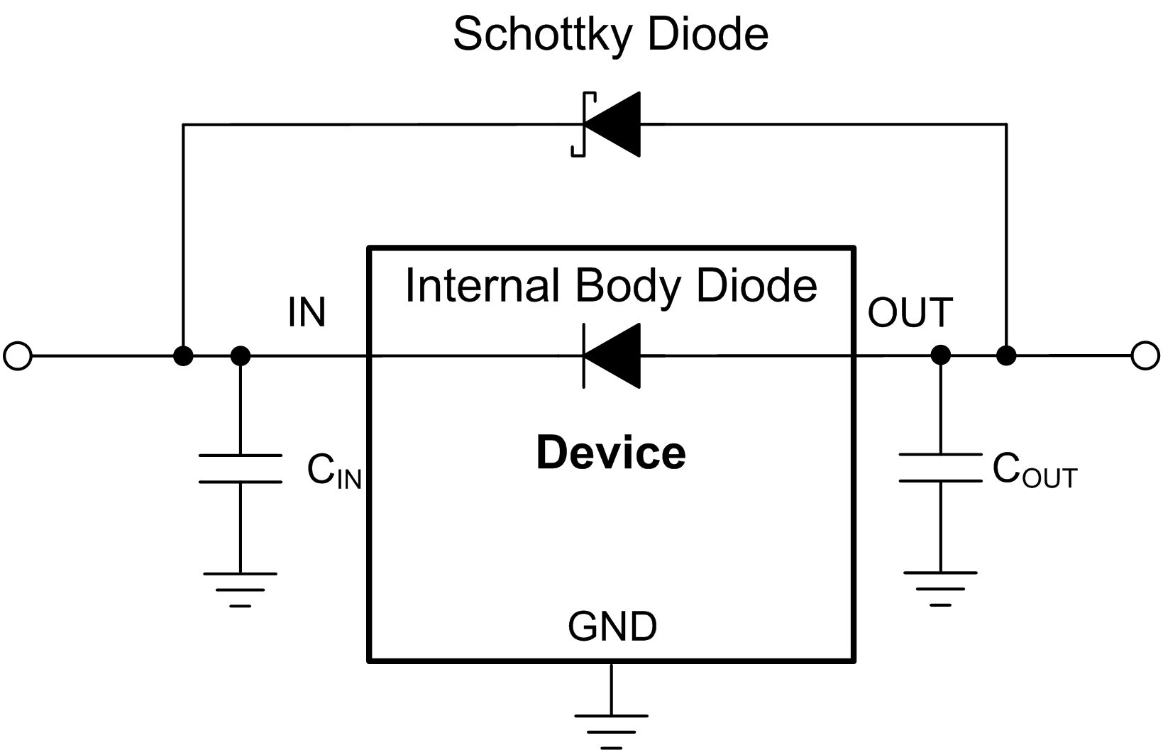
GUID-7E72B42C-F600-4A3A-A3E2-18EECFB41055-low.gif Figure 7-3 Example Circuit for Reverse Current Protection Using a Schottky Diode