SLVS208J May 1999 – August 2015 TPS767
PRODUCTION DATA.
- 1 Features
- 2 Description
- 3 Revision History
- 4 Description (Continued)
- 5 Device Options
- 6 Pin Configuration and Functions
- 7 Specifications
- 8 Parameter Measurement Information
- 9 Detailed Description
- 10Application and Implementation
- 11Layout
- 12Device and Documentation Support
- 13Mechanical, Packaging, and Orderable Information
封装选项
请参考 PDF 数据表获取器件具体的封装图。
机械数据 (封装 | 引脚)
- D|8
- PWP|20
散热焊盘机械数据 (封装 | 引脚)
- PWP|20
订购信息
9 Detailed Description
9.1 Overview
The TPS767xx features very low quiescent current, which remains virtually constant even with varying loads. Conventional LDO regulators use a pnp pass element, the base current of which is directly proportional to the load current through the regulator (IB = IC/β). The TPS767xx uses a PMOS transistor to pass current; because the gate of the PMOS is voltage driven, operating current is low and invariable over the full load range.
Another pitfall associated with the pnp-pass element is its tendency to saturate when the device goes into dropout. The resulting drop in β forces an increase in IB to maintain the load. During power up, this translates to large start-up currents. Systems with limited supply current may fail to start up. In battery-powered systems, it means rapid battery discharge when the voltage decays below the minimum required for regulation. The TPS767xx quiescent current remains low even when the regulator drops out, eliminating both problems.
The TPS767xx family also features a shutdown mode that places the output in the high-impedance state (essentially equal to the feedback-divider resistance) and reduces quiescent current to 2 µA. If the shutdown feature is not used, EN should be tied to ground.
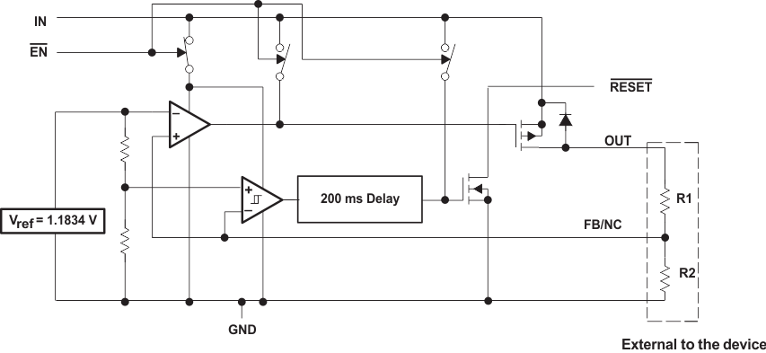
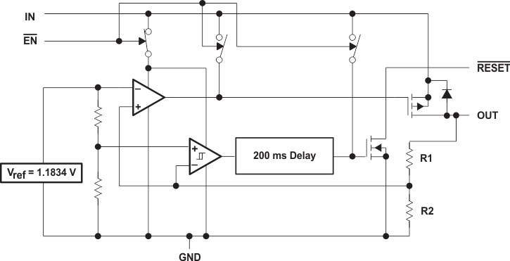
9.2 Functional Block Diagram
 Figure 26. Adjustable Version
 Figure 27. Fixed-Voltage Version
9.3 Feature Description
9.3.1 FB—Pin Connection (adjustable version only)
The FB pin is an input pin to sense the output voltage and close the loop for the adjustable option . The output voltage is sensed through a resistor divider network to close the loop as shown in Figure 28. Normally, this connection should be as short as possible; however, the connection can be made near a critical circuit to improve performance at that point. Internally, FB connects to a high-impedance wide-bandwidth amplifier and noise pickup feeds through to the regulator output. Routing the FB connection to minimize/avoid noise pickup is essential.
9.3.2 Reset Indicator
The TPS767xx features a RESET output that can be used to monitor the status of the regulator. The internal comparator monitors the output voltage: when the output drops to between 92% and 98% of its nominal regulated value, the RESET output transistor turns on, taking the signal low. The open-drain output requires a pullup resistor. If not used, it can be left floating. RESET can be used to drive power-on reset circuitry or as a low-battery indicator. RESET does not assert itself when the regulated output voltage falls outside the specified 2% tolerance, but instead reports an output voltage low relative to its nominal regulated value (refer to Figure 1 timing diagram for start-up sequence).
9.3.3 Regulator Protection
The TPS767xx PMOS-pass transistor has a built-in back diode that conducts reverse currents when the input voltage drops below the output voltage (e.g., during power down). Current is conducted from the output to the input and is not internally limited. When extended reverse voltage is anticipated, external limiting may be appropriate.
The TPS767xx also features internal current limiting and thermal protection. During normal operation, the TPS767xx limits output current to approximately 1.7 A. When current limiting engages, the output voltage scales back linearly until the overcurrent condition ends. While current limiting is designed to prevent gross device failure, care should be taken not to exceed the power dissipation ratings of the package. If the temperature of the device exceeds 150°C(typ), thermal-protection circuitry shuts it down. Once the device has cooled below 130°C(typ), regulator operation resumes.
9.4 Device Functional Modes
9.4.1 Minimum Load Requirements
The TPS767xx family is stable even at zero load; no minimum load is required for operation.
9.5 Programming
9.5.1 Programming the TPS76701 Adjustable LDO Regulator
The output voltage of the TPS76701 adjustable regulator is programmed using an external resistor divider as shown in Figure 28. The output voltage is calculated using:

Where: f = 1.1834 V typ (the internal reference voltage)
Resistors R1 and R2 should be chosen for approximately 50-µA divider current. Lower value resistors can be used but offer no inherent advantage and waste more power. Higher values should be avoided as leakage currents at FB increase the output voltage error. The recommended design procedure is to choose R2 = 30.1 kΩ to set the divider current at 50 µA and then calculate R1 using:

 Figure 28. TPS76701 Adjustable LDO Regulator Programming