SLVS351P September 2002 – March 2015
PRODUCTION DATA.
- 1 Features
- 2 Applications
- 3 Description
- 4 Revision History
- 5 Pin Configuration and Functions
- 6 Specifications
- 7 Detailed Description
- 8 Application and Implementation
- 9 Power Supply Recommendations
- 10Layout
- 11Device and Documentation Support
- 12Mechanical, Packaging, and Orderable Information
封装选项
机械数据 (封装 | 引脚)
散热焊盘机械数据 (封装 | 引脚)
订购信息
8 Application and Implementation
NOTE
Information in the following applications sections is not part of the TI component specification, and TI does not warrant its accuracy or completeness. TI’s customers are responsible for determining suitability of components for their purposes. Customers should validate and test their design implementation to confirm system functionality.
8.1 Application Information
The TPS796xx family of low-dropout (LDO) regulators has been optimized for use in noise-sensitive equipment. The device features extremely low dropout voltages, high PSRR, ultralow output noise, low quiescent current (265 μA typically), and enable input to reduce supply currents to less than 1 μA when the regulator is turned off.
8.2 Typical Application
A typical application circuit is shown in Figure 24.
 Figure 24. Typical Application Circuit
8.2.1 Design Requirements
Table 2 lists the design parameters.
Table 2. Design Parameters
| PARAMETER | DESIGN REQUIREMENT |
|---|---|
| Input voltage | 3.3V |
| Output voltage | 2.5 V |
| Maximum output current | 700 mA |
8.2.2 Detailed Design Procedure
Select the desired device based on the output voltage.
Provide an input supply with adequate headroom to account for dropout and output current to account for the GND terminal current, and power the load.
8.2.2.1 Input and Output Capacitor Requirements
A 2.2-μF or larger ceramic input bypass capacitor, connected between IN and GND and located close to the TPS796xx, is required for stability and improves transient response, noise rejection, and ripple rejection. A higher-value input capacitor may be necessary if large, fast-rise-time load transients are anticipated and the device is located several inches from the power source.
Like most low dropout regulators, the TPS796xx requires an output capacitor connected between OUT and GND to stabilize the internal control loop. The minimum recommended capacitor is 1 μF. Any 1-μF or larger ceramic capacitor is suitable.
8.2.2.2 Output Noise
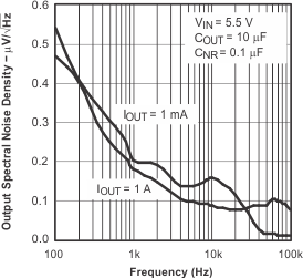
The internal voltage reference is a key source of noise in an LDO regulator. The TPS796xx has an NR pin which is connected to the voltage reference through a 250-kΩ internal resistor. The 250-kΩ internal resistor, in conjunction with an external bypass capacitor connected to the NR pin, creates a low-pass filter to reduce the voltage reference noise and, therefore, the noise at the regulator output. In order for the regulator to operate properly, the current flow out of the NR pin must be at a minimum, because any leakage current creates an IR drop across the internal resistor, thus creating an output error. Therefore, the bypass capacitor must have minimal leakage current. The bypass capacitor should be no more than 0.1 μF in order to ensure that it is fully charged during the quickstart time provided by the internal switch shown in the functional block diagram.
For example, the TPS79630 exhibits 40 μVRMS of output voltage noise using a 0.1-μF ceramic bypass capacitor and a 10-μF ceramic output capacitor. The output starts up slower as the bypass capacitance increases due to the RC time constant at the bypass pin that is created by the internal 250-kΩ resistor and external capacitor.
8.2.2.3 Dropout Voltage
The TPS796 uses a PMOS pass transistor to achieve a low dropout voltage. When (VIN – VOUT) is less than the dropout voltage (VDO), the PMOS pass device is in its linear region of operation and rDS(on) of the PMOS pass element is the input-to-output resistance. Because the PMOS device behaves like a resistor in dropout, VDO approximately scales with the output current.
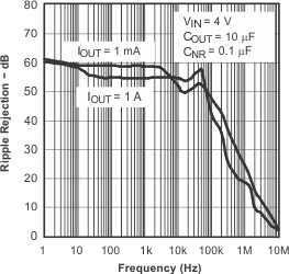
As with any linear regulator, PSRR degrades as (VIN – VOUT) approaches dropout. This effect is illustrated in Figure 9 through Figure 11 in Typical Characteristics.
8.2.2.4 Programming the TPS79601 Adjustable LDO Regulator
The output voltage of the TPS79601 adjustable regulator is programmed using an external resistor divider, as Figure 25 shows.
 Figure 25. Typical Application, Adjustable Output
The output voltage is calculated using Equation 1:

where
- VREF = 1.2246 V typical (the internal reference voltage)
Resistors R1 and R2 should be chosen for approximately 40-μA divider current. Lower value resistors can be used for improved noise performance, but the device wastes more power. Higher values should be avoided, as leakage current at FB increases the output voltage error.
The recommended design procedure is to choose R2 = 30.1 kΩ to set the divider current at 40 μA, C1 = 15 pF for stability, and then calculate R1 using Equation 2:

In order to improve the stability of the adjustable version, it is suggested that a small compensation capacitor be placed between OUT and FB. The approximate value of this capacitor can be calculated as Equation 3:

The suggested value of this capacitor for several resistor ratios is shown in the table in Figure 25. If this capacitor is not used (such as in a unity-gain configuration) then the minimum recommended output capacitor is 2.2 μF instead of 1 μF.
8.2.3 Application Curves
 Figure 26. TPS79630 Output Spectral Noise Density vs Frequency
 Figure 27. TPS79630 Ripple Rejection vs Frequency
8.3 Do's and Don'ts
Place at least one 1-µF ceramic capacitor as close as possible to the OUT pin of the regulator.
Do not place the output capacitor more than 10 mm away from the regulator.
Connect a 2.2-μF low equivalent series resistance (ESR) capacitor across the IN pin and GND input of the regulator.
Do not exceed the absolute maximum ratings.