ZHCSEJ1 December 2015 TPS7H3301-SP
PRODUCTION DATA.
- 1 特性
- 2 应用
- 3 说明
- 4 修订历史记录
- 5 说明 (续)
- 6 Pin Configuration and Functions
- 7 Specifications
- 8 Detailed Description
-
9 Application and Implementation
- 9.1 Application Information
- 9.2
Typical Application
- 9.2.1 Design Requirements
- 9.2.2
Detailed Design Procedure
- 9.2.2.1 VIN/VDD Capacitor
- 9.2.2.2 VLDO Input Capacitor
- 9.2.2.3 VTT Output Capacitor
- 9.2.2.4 VTTSNS Connection
- 9.2.2.5 Low VIN Applications
- 9.2.2.6 S3 and Pseudo-S5 Support
- 9.2.2.7 Tracking Startup and Shutdown
- 9.2.2.8 Output Tolerance Consideration for VTT DIMM Applications
- 9.2.2.9 LDO Design Guidelines
- 9.2.3 Application Curve
- 10Power Supply Recommendations
- 11Layout
- 12器件和文档支持
- 13机械、封装和可订购信息
9 Application and Implementation
NOTE
Information in the following applications sections is not part of the TI component specification, and TI does not warrant its accuracy or completeness. TI’s customers are responsible for determining suitability of components for their purposes. Customers should validate and test their design implementation to confirm system functionality.
9.1 Application Information
The TPS7H3301-SP device is a highly-integrated source sink LDO. The device is targeted to support VTT voltage for DDR memory applications and is capable of sourcing and sinking 3-A load current. The TPS7H3301-SP user’s guide is available on www.ti.com, SLVUAK2. The guide highlights standard EVM test results, schematic, and bill of materials (BOM) for reference.
9.2 Typical Application
The design example describes a 2.5-V Vin, DDR3 configuration.
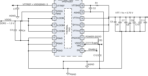 Figure 21. Typical Application Circuit
9.2.1 Design Requirements
See the Recommended Operating Conditions for recommended limits.
9.2.2 Detailed Design Procedure
Table 1. Design Example 1 List of Materials
| REFERENCE DESIGNATOR | DESCRIPTION | SPECIFICATION | PART NUMBER | MANUFACTURER |
|---|---|---|---|---|
| R1 | Resistor | 392 Ω | CRCW0603392RFKEA | |
| R3 | 100 kΩ | CRCW0603100KJNEA | ||
| C3, C5, C6, C7 | Capacitor | 150 µF, 10 V | T530D157M010ATE005 | Kemet |
| C2 | 1000 pF | GRM188R71H102KA01D | MuRata | |
| C1 | 0.1 µF | 08053C104KAT2A | AVX | |
| C4, C8, C9, C10, C11 | 4.7 µF, 10 V | 1210ZC475KAT2A | Murata | |
| C12 | 10 µF, 10 V | GRM21BR71A106KE51L | Murata |
9.2.2.1 VIN/VDD Capacitor
Add a ceramic capacitor, with a value between 1- and 10-μF, placed close to the VIN/VDD pin, to stabilize the bias supply (2.5-V rail or 3.3-V rail) from any parasitic impedance from the supply.
9.2.2.2 VLDO Input Capacitor
Depending on the trace impedance between the VLDOIN/ VDDQ bulk power supply to the device, a transient increase of source current is supplied mostly by the charge from the VLDOIN/ VDDQ input capacitor. Use a 150-μF (or greater) tantalum capacitor in parallel with 4.7uf ceramic capacitor to supply this transient charge. Provide more input capacitance as more output capacitance is used at VO. In general, use one-half of the COUT value for input. One can also determine the input capacitance based upon headroom between VLDOIN and VTT/ Vo voltage differential in the application.
9.2.2.3 VTT Output Capacitor
For stable operation, the total capacitance of the VTT/ Vo output pin must be greater than 470 μF. Attach three, 3 x 150-μF low esr tantalum capacitors in parallel with ceramic capacitors to minimize the effect of equivalent series resistance (ESR) and equivalent series inductance (ESL). If the ESR is greater than 2 mΩ, insert an R-C filter between the output and the VTTSNS input to achieve loop stability. The R-C filter time constant should be almost the same as or slightly lower than the time constant of the output capacitor and its ESR.
9.2.2.4 VTTSNS Connection
To achieve tight regulation with minimum effect of trace resistance, a remote sensing pin, the VTTSNS pin should be connected to the positive pin of the VTT pin output capacitor or capacitors as a separate trace from the high-current path from VTT. Consider adding a low-pass R-C filter at the VTTSNS pin in case the ESR of the VTT output capacitor or capacitors is larger than 2 mΩ. The R-C filter time constant should be approximately the same or slightly lower than the time constant of the VTT output capacitance and ESR.
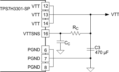 Figure 22. R-C Filter for VTTSNS
9.2.2.5 Low VIN Applications
TPS7H3301-SP can be used in an application system where either a 2.5-V rail or a 3.3-V rail is available. The TPS7H3301-SP minimum input voltage requirement is 2.375 V. If a 2.5-V rail is used, ensure that the absolute minimum voltage (both DC and transient) at the device pin is be 2.375 V or greater. The voltage tolerance for a 2.5-V rail input is between –5% and 5% accuracy, or better.
9.2.2.6 S3 and Pseudo-S5 Support
The TPS7H3301-SP provides S3 support by an EN function. The EN pin could be connected to an SLP_S3 signal in the end application. Both VTTREF and Vo/VTT are on when EN = high (S0 state). VTTREF is maintained while Vo/ VTT is turned off and discharged via an internal discharge MOSFET when EN = low (S3 state). When EN = low and the VDDQSNS voltage is less than 0.780 V, TPS7H3301-SP enters pseudo-S5 state. Both VTTREF and VTTREF outputs are turned off and discharged to GND through internal MOSFETs when pseudo-S5 support is engaged (S4/S5 state). Figure 23 shows a typical startup and shutdown timing diagram for an application that uses S3 and pseudo-S5 support.
9.2.2.7 Tracking Startup and Shutdown
The TPS7H3301-SP also supports tracking startup and shutdown when EN is tied directly to the system bus and not used to turn on or turn off the device. During tracking startup, VO/VTT follows VTTREF once VDDQSNS voltage is greater than 0.78 V. VDDQSNS incorporates the resistor divider network. The typical soft-start time for the VDDQ rail is approximately 3 ms, however it may vary depending on the system configuration. The SS time of the VO/VTT output no longer depends on the OCL setting, but it is a function of the SS time of the VDDQ rail. PGOOD is asserted 2 ms after VO/VTT is within ±20% of VTTREF. During tracking shutdown, VO/VTT falls following VTTREF until VTTREF reaches 0.37 V. Once VTTREF falls below 0.37 V, the internal discharge MOSFETs are turned on and quickly discharge both VTTREF and VO/VTT to GND. PGOOD is deasserted once VO/VTT is beyond the ±20% range of VTTREF. Figure 24 shows the typical timing diagram for an application that uses tracking startup and shutdown.
There are no sequencing requirements between Vin/VDD and VLDOIN. If VLDOIN is applied first followed by VDD/Vin there is no issue. Vin UVLO protection monitors Vin/VDD voltage, when Vin/Vdd is lower than UVLO threshold both VTT and VTTREF regulators are powered off.
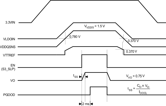 Figure 23. Typical Timing Diagram for S3 and Pseudo-S5 Support
9.2.2.8 Output Tolerance Consideration for VTT DIMM Applications
The TPS7H3301-SP is specifically designed to power up the memory termination rail (as shown in Figure 25). The DDR memory termination structure determines the main characteristics of the VTT rail, which is to be able to sink and source current while maintaining acceptable VTT tolerance. See Figure 26 for typical characteristics for a single memory cell.
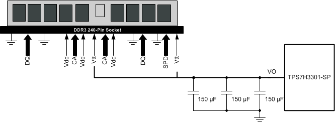 Figure 25. Typical Application Diagram for DDR3 VTT DIMM using TPS7H3301-SP
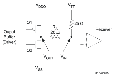 Figure 26. DDR Physical Signal System Bidirectional SSTL Signaling
In Figure 26, when Q1 is on and Q2 is off:
- Current flows from VDDQ via the termination resistor to VTT
- VTT sinks current
In Figure 26, when Q2 is on and Q1 is off:
- Current flows from VTT via the termination resistor to GND
- VTT sources current
Because VTT accuracy has a direct impact on the memory signal integrity, it is imperative to understand the tolerance requirement on VTT. Based on JEDEC VTT specifications for DDR and DDR2 (JEDEC standard: DDR JESD8-9B May 2002; DDR2 JESD8-15A Sept 2003).
VTTREF – 40 mV <VTT <VTTREF + 40 mV, for both dc and ac conditions
The specification itself indicates that VTT must keep track of VTTREF for proper signal conditioning.
The TPS7H3301-SP ensures the regulator output voltage to be:
VTTREF –34 mV <VTT <VTTREF + 34mV, for both DC and AC conditions and –3 A <IVTT <3 A
The regulator output voltage is measured at the regulator side, not the load side. The tolerance is applicable to DDR, DDR2, DDR3 and Low Power DDR3/DDR4 applications (see Table 2 for detailed information). To meet the stability requirement, a minimum output capacitance of 470 μF is needed, combination of both Tantalum and ceramic capacitors. Considering the actual tolerance on the MLCC capacitors, four or higher 4.7-μF ceramic capacitors in parallel with 3 × 150 µF low esr tantalum capacitor are sufficient to meet the above requirement. For higher esr tantalum capacitors it will require multiple tantalum capacitors in parallel with ceramic capacitors to meet system needs.
Table 2. DDR, DDR2, DDR3, and LP DDR3 Termination Technology and Their Differences
| DDR | DDR2 | DDR3 | LOW POWER DDR3 (DDR3L) | |||
|---|---|---|---|---|---|---|
| FSB Data Rates | 200, 266, 333 and 400 MHz | 400, 533, 677 and 800 MHz | 800, 1066, 1330 and 1600 MHz | Same as DDR3 | ||
| Termination | Motherboard termination to VTT for all signals | On-die termination for data group. VTT termination for address, command and control signals | On-die termination for data group. VTT termination for address, command and control signals | Same as DDR3 | ||
| Termination Current Demand | Max source/sink transient currents of up to 2.6 A to 2.9 A | Not as demanding
|
Not as demanding
|
Same as DDR3 | ||
| Voltage Level | 2.5-V Core and I/O 1.25-V VTT | 1.8-V Core and I/O 0.9-V VTT | 1.5-V Core and I/O 0.75-V VTT | 1.35-V Core and I/O 0.68-V VTT | ||
The TPS7H3301-SP is designed as a Gm driven LDO. The voltage droop between the reference input and the output regulator is determined by the transconductance and output current of the device. The typical Gm is 250 S at 3 A and changes with respect to the load in order to conserve the quiescent current (that is, the Gm is very low at no load condition). The Gm LDO regulator is a single pole system. Its unity gain bandwidth for the voltage loop is only determined by the output capacitance, as a result of the bandwidth nature of the Gm (see Equation 1).

where
- FUGBW is the unity gain bandwidth
- Gm is transconductance
- COUT is the output capacitance
There are two limitations to this type of regulator when it comes to the output bulk capacitor requirement. To maintain stability, the zero location contributed by the ESR of the output capacitors should be greater than the –3-dB point of the current loop. This constraint means that higher ESR capacitors should not be used in the design. In addition, the impedance characteristics of the ceramic capacitor should be well understood in order to prevent the gain peaking effect around the Gm –3-dB point because of the large ESL, the output capacitor and parasitic inductance of the VO trace.
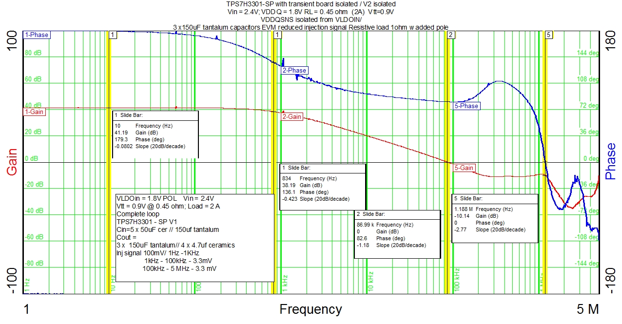
Figure 27 shows the bode plot simulation for a typical DDR3 configuration of the TPS7H3301-SP, where:
- VIN = 2.4 V
- VVLDOIN = 1.5 V
- VVO = 0.75 V
- IIO = 2 A
- 3 × 150-μF low-ESR tantalum capacitors (T530D157M010ATE005) in parallel with 4 × 4.7-µF ceramic capacitor include
- ESR = 1.66 mΩ
- ESL = 800 pH
The unity-gain bandwidth is approximately 87.3 kHz and the phase margin is 82°. The 0-dB level is crossed, the gain peaks because of the ESL effect. However, the peaking is kept well below 0 dB.
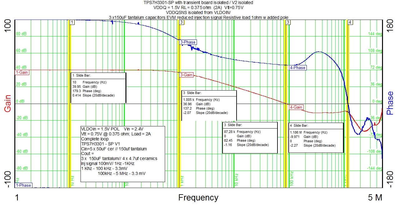 Figure 27. Bode Plot for a Typical DDR3 Configuration
Figure 8 shows the load regulation and Figure 28 shows the transient response for a typical DDR3 configuration. When the regulator is subjected to ±1.5-A load step and release, the output voltage measurement shows no difference between the DC and AC conditions.
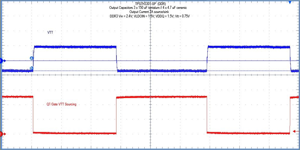 Figure 28. Transient Plot
9.2.2.9 LDO Design Guidelines
The minimum input (VLDOIN) to output voltage (VO/Vtt) difference (headroom) decides the lowest usable supply voltage Gm-driven to drive a certain load. For TPS7H3301-SP, a minimum of 300 mV (VLDOINMIN – VOMAX) is needed in order to support a Gm driven sourcing current of 3 A based on a design of VIN = 3.3 V and C OUT = 470 μF. Because the TPS7H3301-SP is essentially a Gm driven LDO, its impedance characteristics are both a function of the 1/Gm and RDS(on) of the sourcing MOSFET (see Figure 29). The current inflection point of the design is between 3 A and 4 A. When I SRC is less than the inflection point, the LDO is considered to be operating in the Gm region; when ISRC is greater than the inflection point but less than the overcurrent limit point, the LDO is operating in the RDS(on) region. The typical sourcing RDS(on) is 154 mΩ with V IN = 3.0 V and TJ = 125°C.
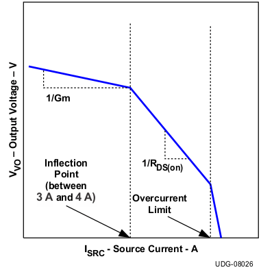 Figure 29. TPS7H3301-SP Impedance Characteristics
9.2.3 Application Curve
