SLVSAI0J October 2010 – May 2016 TPS82670 , TPS82671 , TPS826711 , TPS826716 , TPS82672 , TPS826721 , TPS82673 , TPS82674 , TPS826745 , TPS82675 , TPS82676 , TPS826765 , TPS82677
UNLESS OTHERWISE NOTED, this document contains PRODUCTION DATA.
- 1 Features
- 2 Applications
- 3 Description
- 4 Simplified Schematic
- 5 Revision History
- 6 Device Comparison Table
- 7 Pin Configuration and Functions
- 8 Specifications
- 9 Detailed Description
- 10Applications and Implementation
- 11Power Supply Recommendations
- 12Layout
- 13Device and Documentation Support
- 14Mechanical, Packaging, and Orderable Information
9 Detailed Description
9.1 Overview
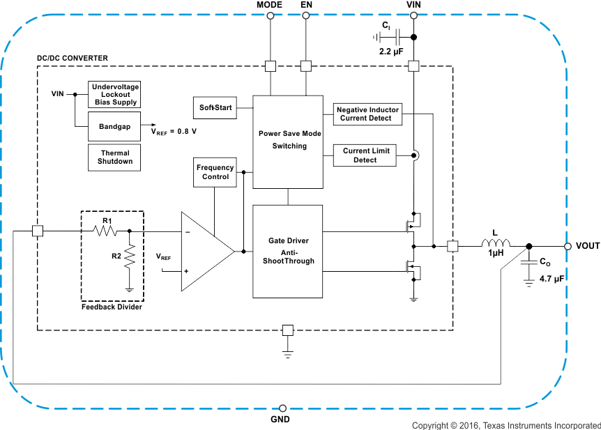
The TPS8267x is a stand-alone, synchronous, step-down converter. The converter operates at a regulated 5.5-MHz frequency pulse width modulation (PWM) at moderate to heavy load currents. At light load currents, the TPS8267x converter operates in power-save mode with pulse frequency modulation (PFM).
The converter uses a unique frequency-locked ring-oscillating modulator to achieve best-in-class load and line response. One key advantage of the non-linear architecture is that there is no traditional feed-back loop. The loop response to change in VO is essentially instantaneous, which explains the transient response. Although this type of operation normally results in a switching frequency that varies with input voltage and load current, an internal frequency lock loop (FLL) holds the switching frequency constant over a large range of operating conditions.
Combined with best-in-class load and line-transient response characteristics, the low quiescent current of the device (approximately 17μA) helps to maintain high efficiency at light load while that current preserves a fast transient response for applications that require tight output regulation.
The TPS8267x integrates an input current limit to protect the device against heavy load or short circuits and features an undervoltage lockout circuit to prevent the device from misoperation at low input voltages. Fully functional operation is permitted down to 2.1V input voltage.
9.2 Functional Block Diagram

9.3 Feature Description
9.3.1 Power-Save Mode
If the load current decreases, the converter enters power-save mode automatically. During power-save mode, the converter operates in discontinuous current, (DCM) single-pulse PFM mode, which produces a low output ripple compared with other PFM architectures.
When in power-save mode, the converter resumes its operation when the output voltage falls below the nominal voltage. The converter ramps up the output voltage with a minimum of one pulse and goes into power-save mode when the output voltage is within its regulation limits.
The IC exits PFM mode and enters PWM mode when the output current can no longer be supported in PFM mode. As a consequence, the DC output voltage is typically positioned approximately 0.5% above the nominal output voltage. The transition between PFM and PWM is seamless.
 Figure 7. Operation In PFM Mode And Transfer To PWM Mode
9.3.2 Mode Selection
The MODE pin selects the operating mode of the device. Connecting the MODE pin to GND enables the automatic PWM and power-save mode operation. The converter operates in regulated frequency PWM mode at moderate to heavy loads, and operates in PFM mode during light loads. This type of operation maintains high efficiency over a wide load current range.
Pulling the MODE pin high forces the converter to operate in PWM mode even at light-load currents. The advantage is that the converter modulates its switching frequency according to a spread spectrum PWM modulation technique that allows simple filtering of the switching harmonics in noise-sensitive applications. In this mode, the efficiency is lower when compared to the power-save mode during light loads.
For additional flexibility, it is possible to switch from power-save mode to PWM mode during operation. This type of operation allows efficient power management by adjusting the operation of the converter to the specific system requirements.
9.3.3 Spread Spectrum, PWM Frequency Dithering
The goal of spread spectrum architecture is to spread out the emitted RF energy over a larger frequency range so that any resulting electromagnetic interference (EMI) is similar to white noise. The end result is a spectrum that is continuous and lower in peak amplitude. Spread spectrum makes it easier to comply with EMI standards. It also makes it easier to comply with the power supply ripple requirements in cellular and non-cellular wireless applications. Radio receivers are typically susceptible to narrowband noise that is focused on specific frequencies.
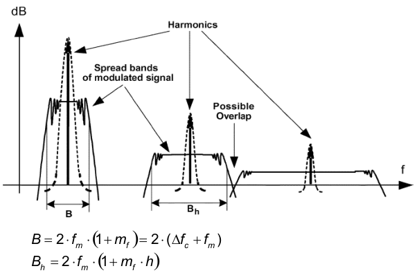
Switching regulators can be particularly troublesome in applications where electromagnetic interference (EMI) is a concern. Switching regulators operate on a cycle-by-cycle basis to transfer power to an output. In most cases, the frequency of operation is either fixed or regulated, based on the output load. This method of conversion creates large components of noise at the frequency of operation (fundamental) and multiples of the operating frequency (harmonics).
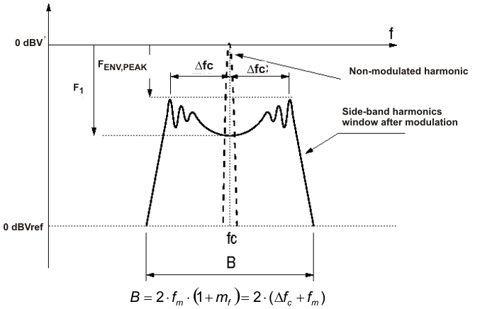
The spread spectrum architecture varies the switching frequency by approximately ±10% of the nominal switching frequency, thereby significantly reduces the peak radiated and conducting noise on both the input and output supplies. The frequency dithering scheme is modulated with a triangle profile and a modulation frequency fm.


Figure 8 and Figure 9 show that after modulation the sideband harmonic is attenuated when compared to the non-modulated harmonic, and when the harmonic energy is spread into a certain frequency band. The higher the modulation index (mf) the larger the attenuation.

With:
fc is the carrier frequency (i.e. nominal switching frequency)
fm is the modulating frequency (approx. 0.016*fc)
δ is the modulation ratio (approx 0.1)

The maximum switching frequency is limited by the process and by the parameter modulation ratio (δ), together with fm, which is the bandwidth of the side-band harmonics around the carrier frequency fc. The bandwidth of a frequency modulated waveform is approximately given by the Carson’s rule and can be summarized as:

fm < RBW: The receiver is not able to distinguish individual side-band harmonics; so, several harmonics are added in the input filter and the measured value is higher than expected in theoretical calculations.
fm > RBW: The receiver is able to properly measure each individual side-band harmonic separately, so that the measurements match the theoretical calculations.
9.4 Device Functional Modes
9.4.1 Enable
The TPS8267x device starts operation when EN is set high and starts up with the soft start as previously described. For proper operation, the EN pin must be terminated and must not be left floating.
Pulling the EN pin low forces the device into shutdown. In this mode, all internal circuits are turned off and the VIN current reduces to the device leakage current, which is typically a few hundred nanoamps.
The TPS8267x device can actively discharge the output capacitor when it turns off. The integrated discharge resistor has a typical resistance of 100 Ω. The required time to ramp down the output voltage depends on the load current and the capacitance present at the output node.
9.4.2 Soft Start
The TPS8267x has an internal soft-start circuit that limits the in-rush current during start-up. This circuit limits input voltage drop when a battery or a high-impedance power source is connected to the input of the MicroSiP™ DC/DC converter.
The soft-start system progressively increases the switching on-time from a minimum pulse-width of 35ns as a function of the output voltage. This mode of operation continues for approximately 100μs after the enable. If the output voltage does not reach its target value within the soft-start time, the soft-start transitions to a second mode of operation.
If the output voltage rises above approximately 0.5V, the converter increases the input current limit and thus enables the power supply to come up properly. The start-up time mainly depends on the capacitance present at the output node and the load current.