SLWS224E August 2010 – January 2016 TRF372017
PRODUCTION DATA.
- 1 Features
- 2 Applications
- 3 Description
- 4 Revision History
- 5 Pin Configuration and Functions
- 6 Specifications
-
7 Detailed Description
- 7.1 Overview
- 7.2 Functional Block Diagram
- 7.3
Feature Description
- 7.3.1 Integer and Fractional Mode Selection
- 7.3.2 Description of PLL Structure
- 7.3.3 Fractional Mode Setup
- 7.3.4 Selecting the VCO and VCO Frequency Control
- 7.3.5 External VCO
- 7.3.6 VCO Test Mode
- 7.3.7 Lock Detect
- 7.3.8 Tx Divider
- 7.3.9 LO Divider
- 7.3.10 Mixer
- 7.3.11 Disabling Outputs
- 7.3.12 Power Supply Distribution
- 7.3.13 Carrier Feedthrough Cancellation
- 7.3.14 Internal Baseband Bias Voltage Generation
- 7.4 Device Functional Modes
- 7.5 Register Maps
- 8 Application and Implementation
- 9 Power Supply Recommendations
- 10Layout
- 11Device and Documentation Support
- 12Mechanical, Packaging, and Orderable Information
7 Detailed Description
7.1 Overview
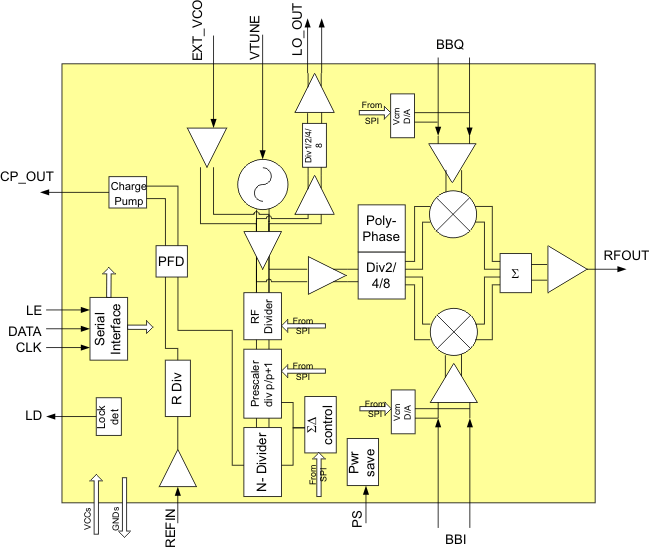
The TRF372017 is a high-performance, direct up-conversion device, integrating a high-linearity, low-noise IQ modulator and an integer-fractional PLL/VCO. The VCO uses integrated frequency dividers to achieve a wide, continuous tuning range of 300 MHz to 4800 MHz. The LO is available as an output with independent frequency dividers. The device also accepts input from an external LO or VCO. The modulator baseband inputs can be biased either internally or externally. Internal DC offset adjustment enables carrier cancellation. The device is controlled through a 3-wire serial programming interface (SPI). A control pin invokes power-save mode to reduce power consumption while keeping the VCO locked for fast start-up.
7.2 Functional Block Diagram
7.3 Feature Description
7.3.1 Integer and Fractional Mode Selection
The PLL is designed to operate in either Integer mode or Fractional mode. If the desired local oscillator (LO) frequency is an integer multiple of the phase frequency detector (PFD) frequency, fPFD, then Integer mode can be selected. The normalized in-band phase noise floor in Integer mode is lower than in Fractional mode. In Integer mode, the feedback divider is an exact integer, and the fraction is zero. While operating in Integer mode, the register bits corresponding to the fractional control are don’t care.
In Fractional mode, the feedback divider fractional portion is non-zero on average. With 25-bit fractional resolution, RF stepsize fPFD/225 is less than 1 Hz with a fPFD up to 33 MHz. The appropriate fractional control bits in the serial register must be programmed.
7.3.2 Description of PLL Structure
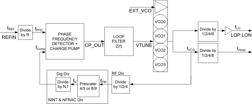 Figure 79. Block Diagram of the PLL Loop
The output frequency is given by Equation 1:

The rate at which phase comparison occurs is fREF/RDIV. In Integer mode, the fractional setting is ignored and Equation 2 is applied.

The feedback divider block consists of a programmable RF divider, a prescaler divider, and an NF divider. The prescaler can be programmed as either a 4/5 or an 8/9 prescaler. The NF divider includes an A counter and an M counter.
7.3.2.1 Selecting PLL Divider Values
Operation of the PLL requires the LO_DIV_SEL, RDIV, PLL_DIV_SEL, NINT, and NFRAC bits to be calculated. The LO or mixer frequency is related to fVCO according to divide-by-1/-2/-4/-8 blocks and the operating range of fVCO.
- LO_DIV_SEL
- PLL_DIV_SEL
- RDIV, NINT, NFRAC, PRSC_SEL

Therefore:

Given fVCO, select the minimum value for PLL_DIV_SEL so that the programmable RF divider limits the input frequency into the prescaler block, fPM, to a maximum of 3000 MHz.
PLL _ DIV _ SEL = min(1, 2, 4) such that fPM ≤ 3000 MHz
This calculation can be restated as Equation 3.

Higher values of fPFD correspond to better phase noise performance in Integer mode or Fractional mode. fPFD, along with PLL_DIV_SEL, determines the fVCO stepsize in Integer mode. Therefore, in Integer mode, select the maximum fPFD that allows for the required RF stepsize, as shown by Equation 4.

In Fractional mode, a small RF stepsize is accomplished through the Fractional mode divider. A large fPFD should be used to minimize the effects of fractional controller noise in the output spectrum. In this case, fPFD may vary according to the reference clock and fractional spur requirements (for example, fPFD = 20 MHz).


The P/(P+1) programmable prescaler is set to 8/9 or 4/5 through the PRSC_SEL bit. To allow proper fractional control, set PRSC_SEL according to Equation 5.

The PRSC_SEL limit at NINT < 75 applies to Fractional mode with third-order modulation. In Integer mode, the PRSC_SEL = 8/9 should be used with NINT as low as 72. The divider block accounts for either value of PRSC_SEL without requiring NINT or NFRAC to be adjusted. Then, calculate the maximum frequency to be input to the digital divider at fN. Use the lower of the possible prescaler divide settings, P = (4,8), as shown by Equation 6.

Verify that the frequency into the digital divider, fN, is less than or equal to 375 MHz. If fN exceeds 375 MHz, choose a larger value for PLL_DIV_SEL and recalculate fPFD, RDIV, NINT, NFRAC, and PRSC_SEL.
7.3.2.2 Setup Example for Integer Mode
Suppose the following operating characteristics are desired for Integer mode operation:
- fREF = 40 MHz (reference input frequency)
- Step at RF = 2 MHz (RF channel spacing)
- fRF = 1600 MHz (RF frequency)
The VCO range is 2400 MHz to 4800 MHz. Therefore:
- LO_DIV_SEL = 2
- fVCO = LO_DIV_SEL × 1600 MHz = 3200 MHz
To keep the frequency of the prescaler less than 3000 MHz:
- PLL_DIV_SEL = 2
The desired stepsize at RF is 2 MHz, so:
- fPFD = 2 MHz
- fVCO, stepsize = PLL_DIV_SEL × fPFD = 4 MHz
Using the reference frequency along with the required fPFD gives:
- RDIV = 20
- NINT = 800
NINT ≥ 75; therefore, select the 8/9 prescaler.
where
This example shows that Integer mode operation gives sufficient resolution for the required stepsize.
7.3.2.3 Setup Example for Fractional Mode
Suppose the following operating characteristics are desired for Fractional mode operation:
- fREF = 40 MHz (reference input frequency)
- Step at RF = 5 MHz (RF channel spacing)
- fRF = 1,600,000,045 Hz (RF frequency)
The VCO range is 2400 MHz to 4800 MHz. Therefore:
- LO_DIV_SEL = 2
- fVCO = LO_DIV_SEL × 1,600,000,045 Hz = 3,200,000,090 Hz
To keep the frequency of the prescaler less than 3000 MHz:
- PLL_DIV_SEL = 2
Using a typical fPFD of 20 MHz:
NINT ≥ 75; therefore, select the 8/9 prescaler.
where
The actual frequency at RF is:
- fRF = 1600000044.9419 Hz
Which yields a frequency error of –0.058 Hz.
7.3.3 Fractional Mode Setup
Optimal operation of the PLL in fractional mode requires several additional register settings. Recommended values are listed in Table 1. Optimal performance may require tuning the MOD_ORD, ISOURCE_SINK, and ISOURCE_TRIM values according to the chosen frequency band.
Table 1. Fractional Mode Register Settings
7.3.4 Selecting the VCO and VCO Frequency Control
To achieve a broad frequency tuning range, the TRF372017 includes four VCOs. Each VCO is connected to a bank of capacitors that determine its valid operating frequency. For any given frequency setting, the appropriate VCO and capacitor array must be selected.
The device contains logic that automatically selects the appropriate VCO and capacitor bank. Set bit EN_CAL to initiate the calibration algorithm. During the calibration process, the device selects a VCO and a capacitor state so that VTune matches the reference voltage set by VCO_CAL_REF_n. Accuracy of the tune is increased through bits CAL_ACC_n. Because a calibration begins immediately when EN_CAL is set, all registers must contain valid values before initiating calibration.
Calibration logic is driven by a CAL_CLK clock derived from the phase frequency detector frequency scaled according to the setting in CAL_CLK_SEL. Faster CAL_CLK frequency enables faster calibration, but the logic is limited to clock frequencies around 1 MHz. Table 2 provides suggested CAL_CLK_SEL scaling recommendations for several phase frequency detector frequencies. The flag R_SAT_ERR is evaluated during the calibration process to indicate calibration counter overflow errors, which occurs if CAL_CLK runs too fast. If R_SAT_ERR is set during a calibration, the resulting calibration is not valid and CAL_CLK_SEL must be used to slow the CAL_CLK. CAL_CLK frequencies should not be set to less than 0.1 MHz.
Table 2. Example CAL_CLK_SEL Scaling
| PFD FREQUENCY (MHz) |
CAL_CLK_SEL SCALING |
CAL_CLK FREQUENCY (MHz) |
|---|---|---|
| 20 | 1/32 | 0.625 |
| 1 | 1 | 1 |
| 0.1 | 8 | 0.8 |
When VCOSEL_MODE is 0, the device automatically selects both the VCO and capacitor bank within 23 CAL_CLK cycles. When VCOSEL_MODE is 1, the device uses the VCO selected in VCO_SEL_0 and VCO_SEL_1 and automatically selects the capacitor array within 17 CAL_CLK cycles. The VCO and capacitor array settings resulting from calibration cannot be read from the VCO_SEL_n and VCO_TRIM_n bits in registers 2 and 7. They can only be read from register 0.
Automatic calibration can be disabled by setting CAL_BYPASS to 1. In this manual cal mode, the VCO is selected through register bits VCO_SEL_n, while the capacitor array is selected through register bits VCO_TRIM_n. Calibration modes are summarized in Table 3. After calibration is complete, the PLL is released from calibration mode to reach an analog lock.
During the calibration process, the TRF372017 scans through many frequencies. RF and LO outputs should be disabled until calibration is complete. At power up, the RF and LO output are disabled by default.
Once a calibration has been performed at a given frequency setting, the calibration is valid over all operating temperature conditions.
Table 3. VCO Calibration Modes
| CAL_BYPASS | VCOSEL_MODE | MAX CYCLES CAL_CLK | VCO | CAPACITOR ARRAY |
|---|---|---|---|---|
| 0 | 0 | 46 | Automatic | |
| 0 | 1 | 34 | VCO_SEL_n | automatic |
| 1 | don't care | na | VCO_SEL_n | VCO_TRIM_n |
7.3.5 External VCO
An external LO or VCO signal may be applied. EN_EXTVCO powers the input buffer and selects the buffered external signal instead of an internal VCO. Dividers, the pfd, and the charge pump remain enabled and may be used to drive an external VCO. NEG_VCO must correspond to the gain of the external VCO.
7.3.6 VCO Test Mode
Setting VCO_TEST_MODE forces the currently selected VCO to the edge of its frequency range by disconnecting the charge pump input from the pfd and loop filter and forcing its output high or low. The upper or lower edge of the VCO range is selected through COUNT_MODE_MUX_SEL.
VCO_TEST_MODE also reports the value of a frequency counter in COUNT, which can be read back in register 0. COUNT reports the number of digital N divider cycles in the PLL, directly related to the period of fN, that occur during each CAL_CLK cycle. Counter operation is initiated through the bit EN_CAL.
Table 4. VCO Test Mode
| VCO_TEST_MODE | COUNT_MODE_MUX_SEL | VCO OPERATION | REGISTER 0 B[30..13] |
|---|---|---|---|
| 0 | don't care | Normal | B[30..24] = undefined
B[23..22] = VCO_SEL selected during autocal B21 = undefined B[20..13] = VCO_TRIM selected during autocal |
| 1 | 0 | Max frequency | B[30..13] = Max frequency counter |
| 1 | 1 | Min frequency | B[30..13] = Min frequency counter |
7.3.7 Lock Detect
The lock detect signal is generated in the phase frequency detector by comparing the VCO target frequency against the VCO actual frequency. When the phase of the two compared frequencies remains aligned for several clock cycles, an internal signal goes high. The precision of this comparison is controlled through the LD_ANA_PREC bits. This internal signal is then averaged and compared against a reference voltage to generate the LD signal. The number of averages used is controlled through LD_DIG_PREC. Therefore, when the VCO is frequency locked, LD is high. When the VCO frequency is not locked, LD may pulse high or exhibit periodic behavior.
By default, the internal lock detect signal is driven on the LD terminal. Register bits MUX_CTRL_n can be used to control a mux to output other diagnostic signals on the LD output. The LD control signals are shown in Table 5.
Table 5. LD Control Signals
| ADJUSTMENT | REGISTER BITS | BIT ADDRESSING |
|---|---|---|
| Lock detect precision | LD_ANA_PREC_0 | Register 4 Bit 19 |
| Unlock detect precision | LD_ANA_PREC_1 | Register 4 Bit 20 |
| LD averaging count | LD_DIG_PREC | Register 4 Bit 24 |
| Diagnostic Output | MUX_CTRL_n | Register 7 Bits 18..16 |
Table 6. LD Control Signal Mode Settings
| CONDITION | RECOMMENDED SETTINGS |
|---|---|
| Integer Mode | LD_ANA_PREC_0 = 0 LD_ANA_PREC_1 = 0 LD_DIG_PREC = 1 |
| Fractional Mode | LD_ANA_PREC_0 = 1 LD_ANA_PREC_1 = 1 LD_DIG_PREC = 1 |
7.3.8 Tx Divider
The Tx divider, illustrated in Figure 80, converts the differential output of the VCO into differential I and Q mixer components. The divide by 1 differential quadrature phases are provided through a polyphase. Divide by 2, 4, and 8 differential quadrature phases are provided through flip-flop dividers. Only one of the dividers operates at a time, and the appropriate output is selected by a mux. DIVn bits are controlled through TX_DIV_SELn.
TX_DIV_I determines the bias level for the divider blocks. The SPEEDUP control is used to bypass a stabilization resistor and reach the final bias level faster after a change in the divider selection. SPEEDUP should be disabled during normal operation.
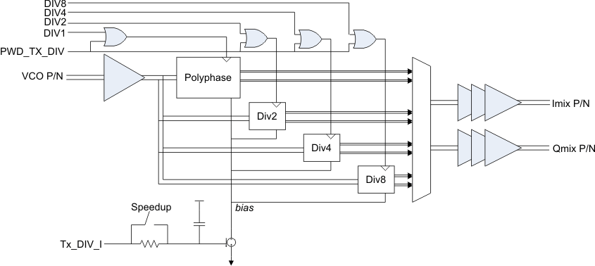 Figure 80. Tx Divider
7.3.9 LO Divider
The LO divider is shown in Figure 81. It frequency divides the VCO output. Only one of the dividers operates at a time, and the appropriate output is selected by a mux. DIVn bits are controlled through LO_DIV_SELn. The output is buffered and provided on output pins LO_OUT_P and LO_OUT_N. The output level is controlled through BUFOUT_BIASn.
LO_DIV_I determines the bias level for the divider blocks. The SPEEDUP control is used to bypass a stabilization resistor and reach the final bias level faster after a change in the divider selection. SPEEDUP should be disabled during normal operation. Although SPEEDUP controls both the Tx and LO divider biases, the Tx and LO divider biases are generated independently.
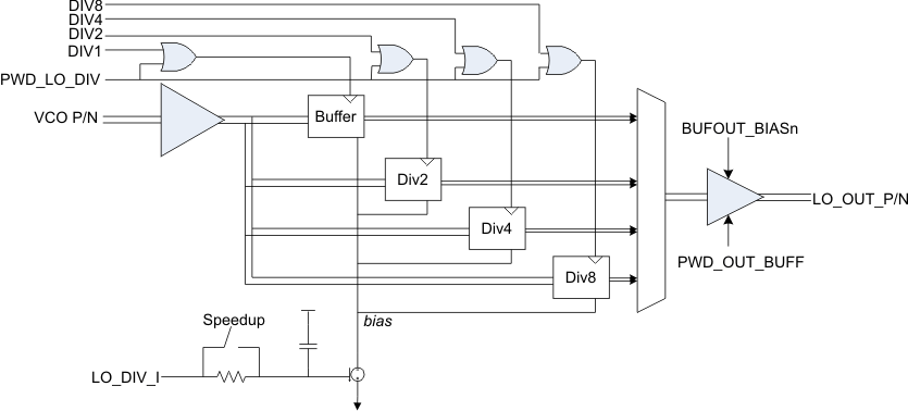 Figure 81. LO Divider
7.3.10 Mixer
A diagram of the mixer is shown in Figure 82. The mixer is followed by a differential to single-ended converter and buffer for output.
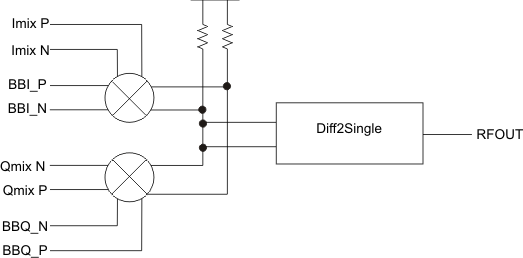 Figure 82. Mixer
7.3.11 Disabling Outputs
RF frequency outputs are generated at the RFOUT and LO* terminals. Unused RF frequency outputs should be disabled to minimize power consumption and noise generation. Table 7 lists settings used to disable the outputs. Power-save mode can also be used to disable outputs.
Table 7. Register Controls for Disabling Outputs
| DISABLED OUTPUT | REGISTER BIT | SETTING |
|---|---|---|
| RFOUT | PWD_TX_DIV | 1 |
| LOP and LON | PWD_OUT_BUFF | 1 |
| PWD_LO_DIV | 1 |
7.3.12 Power Supply Distribution
Power supply distribution for the TRF372017 is shown in Figure 83. Proper isolation and filtering of the supplies is critical for low noise operation of the device. Each supply pin should be supplied with local decoupling capacitance and isolated with a ferrite bead. VCC_VCO2 is tolerant of 5-V supply voltages to permit additional supply filtering.
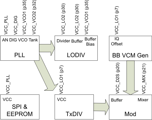 Figure 83. Power Supply Distribution
7.3.13 Carrier Feedthrough Cancellation
The structure of the baseband current DAC is shown in Figure 84. For each input pair, there is a programmable reference current. The reference current for each pair (I and Q) is identical and is programmed through the same register bits, but the reference current source itself is duplicated in the device for both I and Q inputs. This current can be set to change the total current flowing into the P and N nodes, which in turn changes the offset programmability range.
The reference current is then mirrored and multiplied before getting injected into the input node. The total mirrored current is routed into the two sides of the differential pair and routed according to eight programmable bits. As the 8-bit setting is changed, current is shifted from one side of the pair into the other side for each of the I and Q input pairs. In practical usage, the offset current routing distributes the adjustment for each side of the pair, while the reference current sets the range of adjustment. This effect can be seen in Figure 78, which shows that the gain of the current routing is greater when the reference current setting is higher. However the step size also increases with increase in range. Figure 78 shows the effect on common mode voltage of varying the DAC reference current. Adjustment register bits are shown in Table 8.
Offset adjustment may be provided by an external source, such as a DAC QMC block, for DC-coupled systems.
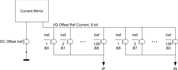 Figure 84. Block Diagram of the Programmable Current DAC
Table 8. Baseband Differential Offset Adjustment Factors
| ADJUSTMENT | REGISTER BITS | BIT ADDRESS |
|---|---|---|
| I input differential offset programmability | I Offset Ref Curr | IOFF_n Register 6 Bits 12..5 |
| Q input differential offset programmability | Q Offset Ref Curr | QOFF Register 6 Bits 20..13 |
| Offset Programmability Range | DCoffset_I_n | Register 7 Bits 30..29 |
7.3.14 Internal Baseband Bias Voltage Generation
The TRF372017 has the ability to generate DC voltage levels for its baseband inputs internally. Register settings in the device allow the user to adjust common mode voltage of the I and Q signals separately. There are three adjustment factors for the baseband inputs. These are described in Table 9.
Table 9. Baseband Adjustment Factors
| ADJUSTMENT | REGISTER BITS | BIT ADDRESSING |
|---|---|---|
| VCM setting | VREF_SEL_n | Register 6 Bits 23..21 |
| VCM Enable | PWD_BB_VCM | Register 4 Bit 15 |
| Bias select | IB_VCM_SEL | Register 7 Bit 25 |
Each baseband input pair includes the circuitry depicted in Figure 85. The Vref set voltage impacts all four terminals: IP, IN, QP, and QN. The effect of changing the reference voltage is shown in Figure 77. Each node also includes a programmable current DAC that injects current into the positive and negative terminals of each input.
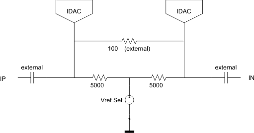 Figure 85. Block Diagram of the Baseband I Input Nodes
Table 10. Frequency Range Operation
| VCO FREQUENCY | DIV BY 2 | DIV BY 4 | DIV BY 8 | ||||
|---|---|---|---|---|---|---|---|
| Fmin | Fmax | Fmin | Fmax | Fmin | Fmax | Fmin | Fmax |
| 2400 | 4800 | 1200 | 2400 | 600 | 1200 | 300 | 600 |
7.4 Device Functional Modes
7.4.1 Powersave Mode
Powersave mode can be used to put the device into a low power consumption mode. The PLL block remains active in Powersave mode, reducing the time required for start-up. However, the modulator, dividers, output buffers, and baseband common mode generation blocks are powered down. The SPI block remains active, and registers are addressable. Use the PS pin to activate powersave mode.
7.5 Register Maps
7.5.1 Serial Interface Programming Registers Definition
The TRF372017 features a 3-wire serial programming interface (SPI) that controls an internal 32-bit shift register. There are a total of 3 signals that must be applied: the clock (CLK, pin 47), the serial data (DATA, pin 46) and the latch enable (LE, pin 45). The TRF372017 has an additional pin (RDBK, pin 2) for read-back functionality. This pin is a digital pin and can be used to read-back values of different internal registers.
The DATA (DB0-DB31) is loaded LSB first and is read on the rising edge of the CLOCK. The LE is asynchronous to the CLOCK and at its rising edge the data in the shift register gets loaded onto the selected internal register. The 5 LSB of the Data field are the address bits to select the available internal registers.
7.5.1.1 PLL SPI Registers
7.5.1.1.1 Register 1
Table 1. Register 1
| Bit0 | Bit1 | Bit2 | Bit3 | Bit4 | Bit5 | Bit6 | Bit7 | Bit8 | Bit9 | Bit10 | Bit11 | Bit12 | Bit13 | Bit14 | Bit15 |
| Register address | Reference Clock Divider | ||||||||||||||
| Bit16 | Bit17 | Bit18 | Bit19 | Bit20 | Bit21 | Bit22 | Bit23 | Bit24 | Bit25 | Bit26 | Bit27 | Bit28 | Bit29 | Bit30 | Bit31 |
| …. | RSV | REF INV | VCO NEG | Charge Pump Current | CP DOUBLE | VCO Cal CLK div/Mult | RSV | ||||||||
Table 11. Register 1 Field Descriptions
CAL_CLK_SEL[3..0]: Set the frequency divider value used to derive the VCO calibration clock from the phase detector frequency.
Table 12. Scaling Factors
| CAL_CLK_SEL | SCALING FACTOR |
|---|---|
| 1111 | 1/128 |
| 1110 | 1/64 |
| 1101 | 1/32 |
| 1100 | 1/16 |
| 1011 | 1/8 |
| 1010 | 1/4 |
| 1001 | ½ |
| 1000 | 1 |
| 0110 | 2 |
| 0101 | 4 |
| 0100 | 8 |
| 0011 | 16 |
| 0010 | 32 |
| 0001 | 64 |
| 0000 | 128 |
ICP[4..0]: Set the charge pump current.
Table 13. ICP and Current
| ICP[4..0] | CURRENT (mA) |
|---|---|
| 00 000 | 1.94 |
| 00 001 | 1.76 |
| 00 010 | 1.62 |
| 00 011 | 1.49 |
| 00 100 | 1.38 |
| 00 101 | 1.29 |
| 00 110 | 1.21 |
| 00 111 | 1.14 |
| 01 000 | 1.08 |
| 01 001 | 1.02 |
| 01 010 | 0.97 |
| 01 011 | 0.92 |
| 01 100 | 0.88 |
| 01 101 | 0.84 |
| 01 110 | 0.81 |
| 01 111 | 0.78 |
| 10 000 | 0.75 |
| 10 001 | 0.72 |
| 10 010 | 0.69 |
| 10 011 | 0.67 |
| 10 100 | 0.65 |
| 10 101 | 0.63 |
| 10 110 | 0.61 |
| 10 111 | 0.59 |
| 11 000 | 0.57 |
| 11 001 | 0.55 |
| 11 010 | 0.54 |
| 11 011 | 0.52 |
| 11 100 | 0.51 |
| 11 101 | 0.5 |
| 11 110 | 0.48 |
| 11 111 | 0.47 |
7.5.1.1.2 Register 2
Table 2. Register 2
| Bit0 | Bit1 | Bit2 | Bit3 | Bit4 | Bit5 | Bit6 | Bit7 | Bit8 | Bit9 | Bit10 | Bit11 | Bit12 | Bit13 | Bit14 | Bit15 |
| Register address | N-Divider Value | ||||||||||||||
| Bit16 | Bit17 | Bit18 | Bit19 | Bit20 | Bit21 | Bit22 | Bit23 | Bit24 | Bit25 | Bit26 | Bit27 | Bit28 | Bit29 | Bit30 | Bit31 |
| ... | PLL divider setting | Prescaler Select | RSV | RSV | VCO select | FCO sel mode | Cal accuracy | CAL | |||||||
Table 14. Register 2 Field Descriptions
PLL_DIV<1,0>: Select division ratio of divider in front of prescaler.
Table 15. Frequency Divider
| PLL DIV | FREQUENCY DIVIDER |
|---|---|
| 00 | 1 |
| 01 | 2 |
| 10 | 4 |
VCOSEL_MODE<0>: When it is 1, the cap array calibration is run on the VCO selected through bits VCO_SEL<2,1>.
7.5.1.1.3 Register 3
Table 3. Register 3
| Bit0 | Bit1 | Bit2 | Bit3 | Bit4 | Bit5 | Bit6 | Bit7 | Bit8 | Bit9 | Bit10 | Bit11 | Bit12 | Bit13 | Bit14 | Bit15 |
| Register address | Fractional N-Divider Value | ||||||||||||||
| Bit16 | Bit17 | Bit18 | Bit19 | Bit20 | Bit21 | Bit22 | Bit23 | Bit24 | Bit25 | Bit26 | Bit27 | Bit28 | Bit29 | Bit30 | Bit31 |
| ... | RSV | RSV | |||||||||||||
Table 16. Register 3 Field Descriptions
| REGISTER 3 | NAME | RESET VALUE | DESCRIPTION |
|---|---|---|---|
| Bit0 | ADDR_0 | 1 | Register address bits |
| Bit1 | ADDR_1 | 1 | |
| Bit2 | ADDR_2 | 0 | |
| Bit3 | ADDR_3 | 1 | |
| Bit4 | ADDR_4 | 0 | |
| Bit5 | NFRAC<0> | 0 | Fractional PLL N divider value 0 to 0.99999. |
| Bit6 | NFRAC<1> | 0 | |
| Bit7 | NFRAC<2> | 0 | |
| Bit8 | NFRAC<3> | 0 | |
| Bit9 | NFRAC<4> | 0 | |
| Bit10 | NFRAC<5> | 0 | |
| Bit11 | NFRAC<6> | 0 | |
| Bit12 | NFRAC<7> | 0 | |
| Bit13 | NFRAC<8> | 0 | |
| Bit14 | NFRAC<9> | 0 | |
| Bit15 | NFRAC<10> | 0 | |
| Bit16 | NFRAC<11> | 0 | |
| Bit17 | NFRAC<12> | 0 | |
| Bit18 | NFRAC<13> | 0 | |
| Bit19 | NFRAC<14> | 0 | |
| Bit20 | NFRAC<15> | 0 | |
| Bit21 | NFRAC<16> | 0 | |
| Bit22 | NFRAC<17> | 0 | |
| Bit23 | NFRAC<18> | 0 | |
| Bit24 | NFRAC<19> | 0 | |
| Bit25 | NFRAC<20> | 0 | |
| Bit26 | NFRAC<21> | 0 | |
| Bit27 | NFRAC<22> | 0 | |
| Bit28 | NFRAC<23> | 0 | |
| Bit29 | NFRAC<24> | 0 | |
| Bit30 | RSV | 0 | |
| Bit31 | RSV | 0 |
7.5.1.1.4 Register 4
Table 4. Register 4
| Bit0 | Bit1 | Bit2 | Bit3 | Bit4 | Bit5 | Bit6 | Bit7 | Bit8 | Bit9 | Bit10 | Bit11 | Bit12 | Bit13 | Bit14 | Bit15 |
| Register address | PD PLL | Power-Down PLL blocks | PD VCM | ||||||||||||
| Bit16 | Bit17 | Bit18 | Bit19 | Bit20 | Bit21 | Bit22 | Bit23 | Bit24 | Bit25 | Bit26 | Bit27 | Bit28 | Bit29 | Bit30 | Bit31 |
| PD DC off | EXT VCO | PLL Test Control | ΣΔ Mode order | ΣΔ Mode controls | EN Fract mode | ||||||||||
Table 17. Register 4 Field Descriptions
| REGISTER 4 | NAME | RESET VALUE | DESCRIPTION |
|---|---|---|---|
| Bit0 | ADDR_0 | 0 | Register address bits |
| Bit1 | ADDR_1 | 0 | |
| Bit2 | ADDR_2 | 1 | |
| Bit3 | ADDR_3 | 1 | |
| Bit4 | ADDR_4 | 0 | |
| Bit5 | PWD_PLL | 0 | Power-down all PLL blocks (1 = off) |
| Bit6 | PWD_CP | 0 | When 1, charge pump is off |
| Bit7 | PWD_VCO | 0 | When 1, VCO is off |
| Bit8 | PWD_VCOMUX | 0 | Power-down the 4 VCO mux block (1 = Off) |
| Bit9 | PWD_DIV124 | 0 | Power-down programmable RF divider in PLL feedback path (1 = off) |
| Bit10 | PWD_PRESC | 0 | Power-down programmable prescaler (1 = off) |
| Bit11 | RSV | 0 | |
| Bit12 | PWD_OUT_BUFF | 1 | Power-down LO output buffer (1 = off). |
| Bit13 | PWD_LO_DIV | 1 | Power-down frequency divider in LO output chain 1 (1 = off) |
| Bit14 | PWD_TX_DIV | 1 | Power-down frequency divider in modulator chain (1 = off) |
| Bit15 | PWD_BB_VCM | 1 | Power-down baseband input DC common block (1 = off) |
| Bit16 | PWD_DC_OFF | 1 | Power-down baseband input DC offset control block (1 = off) |
| Bit17 | EN_EXTVCO | 0 | Enable external LO/VCO input buffer (1 = enabled) |
| Bit18 | EN_ISOURCE | 0 | Enable offset current at Charge Pump output (to be used in fractional mode only, 1 = on). |
| Bit19 | LD_ANA_PREC_0 | 0 | Control precision of analog lock detector (1 1 = low; 0 0 = high). See Lock Detect section of Application Information for usage details. |
| Bit20 | LD_ANA_PREC_1 | 0 | |
| Bit21 | CP_TRISTATE_0 | 0 | Set the charge pump output in Tristate mode. Normal, B[22..21] = [00] Down, B[22..21] = [01] Up, B[22..21] = [10] Tristate, B[22..21] = [11] |
| Bit22 | CP_TRISTATE_1 | 0 | |
| Bit23 | SPEEDUP | 0 | Speed up PLL and Tx blocks by bypassing bias stabilizer capacitors. |
| Bit24 | LD_DIG_PREC | 0 | Lock detector precision (increases sampling time if set to 1) |
| Bit25 | EN_DITH | 1 | Enable ΔΣ modulator dither (1=on) |
| Bit26 | MOD_ORD_0 | 0 | ΔΣ modulator order (1 through 4). Not used in integer mode. 1st order, B[27..26] = [00] 2nd order, B[27..26] = [01] 3rd order, B[27..26] = [10] 4th order, B[27..26] = [11] |
| Bit27 | MOD_ORD_1 | 1 | |
| Bit28 | DITH_SEL | 0 | Select dither mode for ΔΣ modulator (0 = const; 1 = pseudo-random) |
| Bit29 | DEL_SD_CLK_0 | 0 | ΔΣ modulator clock delay. Not used in integer mode. Min delay = 00 Max delay = 11 |
| Bit30 | DEL_SD_CLK_1 | 1 | |
| Bit31 | EN_FRAC | 0 | Enable fractional mode (1 = fractional enabled) |
7.5.1.1.5 Register 5
Table 5. Register 5
| Bit0 | Bit1 | Bit2 | Bit3 | Bit4 | Bit5 | Bit6 | Bit7 | Bit8 | Bit9 | Bit10 | Bit11 | Bit12 | Bit13 | Bit14 | Bit15 |
| Register address | VCO_R Trim | PLL_R_Trim | VCO Current | VCOBUF BIAS | |||||||||||
| Bit16 | Bit17 | Bit18 | Bit19 | Bit20 | Bit21 | Bit22 | Bit23 | Bit24 | Bit25 | Bit26 | Bit27 | Bit28 | Bit29 | Bit30 | Bit31 |
| VCOMUX BIAS | OUTBUF BIAS | RSV | BIAS SEL | VCO CAL REF | VCOMUX AMPL | VCO Bias Voltage | RSV | EN_LD ISRC | |||||||
Table 18. Register 5 Field Descriptions
| REGISTER 5 | NAME | RESET VALUE | DESCRIPTION |
|---|---|---|---|
| Bit0 | ADDR_0 | 1 | Register address bits |
| Bit1 | ADDR_1 | 0 | |
| Bit2 | ADDR_2 | 1 | |
| Bit3 | ADDR_3 | 1 | |
| Bit4 | ADDR_4 | 0 | |
| Bit5 | VCOBIAS_RTRIM_0 | 0 | VCO bias resistor trimming. Recommended programming [100]. |
| Bit6 | VCOBIAS_RTRIM_1 | 0 | |
| Bit7 | VCOBIAS_RTRIM_2 | 1 | |
| Bit8 | PLLBIAS_RTRIM_0 | 0 | PLL bias resistor trimming. Recommended programming [10]. |
| Bit9 | PLLBIAS_RTRIM_1 | 1 | |
| Bit10 | VCO_BIAS_0 | 0 | VCO bias reference current. 300 µA, B[13..10] = [00 00] 600 µA, B[13..10] = [11 11] Bias current varies directly with reference current Recommended programming 400 µA, B[13..10] = [0101] with VCC_VCO2 = 3.3 V 600 µA, B[13..10] = [1111] with VCC_VCO2 = 5 V |
| Bit11 | VCO_BIAS_1 | 0 | |
| Bit12 | VCO_BIAS_2 | 0 | |
| Bit13 | VCO_BIAS_3 | 1 | |
| Bit14 | VCOBUF_BIAS_0 | 0 | VCO buffer bias reference current. 300 µA, B[15..14] = [00] 600 µA, B[15..14] = [11] Bias current varies directly with reference current Recommended programming [10] |
| Bit15 | VCOBUF_BIAS_1 | 1 | |
| Bit16 | VCOMUX_BIAS_0 | 0 | VCO’s muxing buffer bias reference current. 300 µA, B[17..16] = [00] 600 µA, B[17..16] = [11] Bias current varies directly with reference current Recommended programming [11] |
| Bit17 | VCOMUX_BIAS_1 | 1 | |
| Bit18 | BUFOUT_BIAS_0 | 0 | PLL output buffer bias reference current. 300 µA, B[19..18] = [00] 600 µA, B[19..18] = [11] Bias current varies directly with reference current |
| Bit19 | BUFOUT_BIAS_1 | 1 | |
| Bit20 | RSV | 0 | |
| Bit21 | RSV | 1 | |
| Bit22 | VCO_CAL_IB | 0 | Select bias current type for VCO calibration circuitry 0 = PTAT; 1 = constant over temperature Recommended programming [0] |
| Bit23 | VCO_CAL_REF_0 | 0 | VCO calibration reference voltage trimming. 0.9 V, B[25..23] = [000] 1.4 V, B[25..23] = [111] Recommended programming [010] |
| Bit24 | VCO_CAL_REF_1 | 0 | |
| Bit25 | VCO_CAL_REF_2 | 1 | |
| Bit26 | VCO_AMPL_CTRL_0 | 0 | Adjust the signal amplitude at the VCO mux input Recommended programming [11] |
| Bit27 | VCO_AMPL_CTRL_1 | 1 | |
| Bit28 | VCO_VB_CTRL_0 | 0 | VCO core bias voltage control 1.2 V, B[29..28] = [00] 1.35 V, B[29..28] = [01] 1.5 V, B[29..28] = [10] 1.65 V, B[29..28] = [11] Recommended programming [00] |
| Bit29 | VCO_VB_CTRL _1 | 1 | |
| Bit30 | RSV | 0 | |
| Bit31 | EN_LD_ISOURCE | 1 | Enable monitoring of LD to turn on Isource when in frac-n mode (EN_FRAC=1). 0 = ISource set by EN_ISOURCE. 1 = ISource set by LD. Recommended programming [0] |
7.5.1.1.6 Register 6
Table 6. Register 6
| Bit0 | Bit1 | Bit2 | Bit3 | Bit4 | Bit5 | Bit6 | Bit7 | Bit8 | Bit9 | Bit10 | Bit11 | Bit12 | Bit13 | Bit14 | Bit15 |
| Register address | BB DC OFFSET | ||||||||||||||
| Bit16 | Bit17 | Bit18 | Bit19 | Bit20 | Bit21 | Bit22 | Bit23 | Bit24 | Bit25 | Bit26 | Bit27 | Bit28 | Bit29 | Bit30 | Bit31 |
| BB DC OFFSET | VREF SEL | TXDIV SEL | LODIV SEL | TXDIV BIAS | LODIV BIAS | ||||||||||
Table 19. Register 6 Field Descriptions
| REGISTER 6 | NAME | RESET VALUE | DESCRIPTION |
|---|---|---|---|
| Bit0 | ADDR_0 | 0 | Register address bits |
| Bit1 | ADDR_1 | 1 | |
| Bit2 | ADDR_2 | 1 | |
| Bit3 | ADDR_3 | 1 | |
| Bit4 | ADDR_4 | 0 | |
| Bit5 | IOFF_0 | 0 | Adjust Iref current used for defining I DC offset. Full range, 2 × Iref, B[12..5] = [1 1111 111] Mid scale, Iref B[12..5] = [1 0000 000] |
| Bit6 | IOFF_1 | 0 | |
| Bit7 | IOFF_2 | 0 | |
| Bit8 | IOFF_3 | 0 | |
| Bit9 | IOFF_4 | 0 | |
| Bit10 | IOFF_5 | 0 | |
| Bit11 | IOFF_6 | 0 | |
| Bit12 | IOFF_7 | 1 | |
| Bit13 | QOFF_0 | 0 | Adjust Iref current used for defining Q DC offset. Full range, 2 × Iref, B[20..13] = [1 1111 111] Mid scale, Iref B[20..13] = [1 0000 000] |
| Bit14 | QOFF_1 | 0 | |
| Bit15 | QOFF_2 | 0 | |
| Bit16 | QOFF_3 | 0 | |
| Bit17 | QOFF_4 | 0 | |
| Bit18 | QOFF_5 | 0 | |
| Bit19 | QOFF_6 | 0 | |
| Bit20 | QOFF_7 | 1 | |
| Bit21 | VREF_SEL_0 | 0 | Adjust Vref in baseband common mode generation circuit. 0.65 V, B[23..21] = [000] 1 V, B[23..21] = [111] Modulator common mode is Vref + Vbe. Recommended programming [100] |
| Bit22 | VREF_SEL_1 | 0 | |
| Bit23 | VREF_SEL_2 | 1 | |
| Bit24 | TX_DIV_SEL_0 | 0 | Adjust Tx path divider. Div1, [B25..24] = [00] Div2, [B25..24] = [01] Div4, [B25..24] = [10] Div8, [B25..24] = [11] |
| Bit25 | TX_DIV_SEL_1 | 0 | |
| Bit26 | LO_DIV_SEL_0 | 0 | Adjust LO path divider Div1, [B28..27] = [00] Div2, [B28..27] = [01] Div4, [B28..27] = [10] Div8, [B28..27] = [11] |
| Bit27 | LO_DIV_SEL_1 | 0 | |
| Bit28 | TX_DIV_BIAS_0 | 0 | TX divider bias reference current 25 µA, [B29..28] = [00] 37.5 µA, [B29..28] = [01] 50 µA, [B29..28] = [10] 62.5 µA, [B29..28] = [11] Bias current varies directly with reference current |
| Bit29 | TX_DIV_BIAS_1 | 1 | |
| Bit30 | LO_DIV_BIAS_0 | 0 | LO divider bias reference current 25 µA, [B29..28] = [00] 37.5 µA, [B29..28] = [01] 50 µA, [B29..28] = [10] 62.5 µA, [B29..28] = [11] Bias current varies directly with reference current |
| Bit31 | LO_DIV_BIAS_1 | 1 |
7.5.1.1.7 Register 7
Table 7. Register 7
| Bit0 | Bit1 | Bit2 | Bit3 | Bit4 | Bit5 | Bit6 | Bit7 | Bit8 | Bit9 | Bit10 | Bit11 | Bit12 | Bit13 | Bit14 | Bit15 |
| Register address | VCO CAP ARRAY CONTROL | RSV | VCO test mode | CAL bypass | |||||||||||
| Bit16 | Bit17 | Bit18 | Bit19 | Bit20 | Bit21 | Bit22 | Bit23 | Bit24 | Bit25 | Bit26 | Bit27 | Bit28 | Bit29 | Bit30 | Bit31 |
| MUX CONTROL | ISRC SINK | OFFSET CURRENT ADJUST | LP PD TimeConst | VCM Bias | MIX LO VCM | DC OFF REF | VCO BIAS SEL | ||||||||
Table 20. Register 7 Field Descriptions
| REGISTER 7 | NAME | RESET VALUE | DESCRIPTION |
|---|---|---|---|
| Bit0 | ADDR_0 | 1 | Register address bits |
| Bit1 | ADDR_1 | 1 | |
| Bit2 | ADDR_2 | 1 | |
| Bit3 | ADDR_3 | 1 | |
| Bit4 | ADDR_4 | 0 | |
| Bit5 | RSV | 0 | |
| Bit6 | RSV | 0 | |
| Bit7 | VCO_TRIM_0 | 0 | VCO capacitor array control bits, used in manual cal mode |
| Bit8 | VCO_TRIM_1 | 0 | |
| Bit9 | VCO_TRIM_2 | 0 | |
| Bit10 | VCO_TRIM_3 | 0 | |
| Bit11 | VCO_TRIM_4 | 0 | |
| Bit12 | VCO_TRIM_5 | 1 | |
| Bit13 | RSV | 0 | |
| Bit14 | VCO_TEST_MODE | 0 | Counter mode: measure max/min frequency of each VCO |
| Bit15 | CAL_BYPASS | 0 | Bypass of VCO auto-calibration. When 1, VCO_TRIM and VCO_SEL bits are used to select the VCO and the cap array setting |
| Bit16 | MUX_CTRL_0 | 1 | Select signal for test output (pin 5, LD). [000] = Ground [001] = Lock detector [010] = NDIV counter output [011] = Ground [100] = RDIV counter output [101] = Ground [110] = A_counter output [111] = Logic high; |
| Bit17 | MUX_CTRL_1 | 0 | |
| Bit18 | MUX_CTRL_2 | 0 | |
| Bit19 | ISOURCE_SINK | 0 | Charge pump offset current polarity. |
| Bit20 | ISOURCE_TRIM_0 | 0 | Adjust isource bias current in frac-n mode. |
| Bit21 | ISOURCE_TRIM_1 | 0 | |
| Bit22 | ISOURCE_TRIM_2 | 1 | |
| Bit23 | PD_TC_0 | 0 | Time constant control for PWD_OUT_BUFF [00] = Minimum time constant [11] = Maximum time constant |
| Bit24 | PD_TC_1 | 0 | |
| Bit25 | IB_VCM_SEL | 0 | Select constant/ptat current for Common mode bias generation block 0 = PTAT 1 = const |
| Bit26 | RSV | 0 | |
| Bit27 | RSV | 0 | |
| Bit28 | RSV | 1 | |
| Bit29 | DCOFFSET_I_0 | 0 | Adjust BB input DC offset Iref 50 µA, B[27..26] = [00] 100 µA, B[27..26] = [01] 150 µA, B[27..26] = [10] 200 µA, B[27..26] = [11] |
| Bit30 | DCOFFSET_I_1 | 1 | |
| Bit31 | VCO_BIAS_SEL | 0 | Select VCO_BIAS trim settings stored in EEPROM 0 = Use EEPROM settings if parity check is 1; otherwise, use SPI settings 1 = Use SPI settings Recommended programming [1] |
7.5.1.2 Readback Mode
Register 0 functions as a Readback register. TRF372017 implements the capability to read-back the content of any serial programming interface register by initializing register 0.
Each read-back is composed by two phases: writing followed by the actual reading of the internal data. This is shown in the timing diagram in Figure 2. During the writing phase, a command is sent to TRF372017 register 0 to set it in read-back mode and to specify which register is to be read. In the proper reading phase, at each rising clock edge, the internal data is transferred into the RDBK pin and can be read at the following falling edge (LSB first). The first clock after the LE goes high (end of writing cycle) is idle and the following 32 clocks pulses transfer the internal register content to the RDBK pin.
7.5.1.2.1 Readback From the Internal Registers Banks
TRF372017 integrates 8 registers: Register 0 (000) to Register 7 (111). Registers 1 through 7 are used to set-up and control the TRF372017 functionalities, while register 0 is used for the readback function.
The latter register must be programmed with a specific command that sets TRF372017 in read-back mode and specifies the register to be read:
- Set B[31] to 1 to put TRF372017 in read-back mode.
- Set B[30,28] equal to the address of the register to be read (000 to 111).
- Set B27 to control the VCO frequency counter in VCO test mode.
7.5.1.2.1.1 Register 0 Write
Table 21. Register 0 Write
The contents of any register specified in RB_REG can be read back during the read cycle, including register 0.
| Bit0 | Bit1 | Bit2 | Bit3 | Bit4 | Bit5 | Bit6 | Bit7 | Bit8 | Bit9 | Bit10 | Bit11 | Bit12 |
| Register address | CHIP_ID | NU | R_SAT_ERR | |||||||||
| Bit13 | Bit14 | Bit15 | Bit16 | Bit17 | Bit18 | Bit19 | Bit20 | Bit21 | Bit22 | Bit23 | Bit24 | Bit25 | Bit26 | Bit27 | Bit28 | Bit29 | Bit30 |
| COUNT0-7/VCO_TRM | COUNT8-10/VCO_SEL | COUNT11-17 | |||||||||||||||
| Bit31 |
| COUNT_MODE-MUX-SEL |