ZHCSDL6C November 2014 – March 2019 TS3DDR4000
PRODUCTION DATA.
11.1 Layout Guidelines
Standard layout technique for 0.65 mm pitch BGA package shall be employed. The following commonly-used printed-circuit-board (PCB) layout guidelines are recommended:
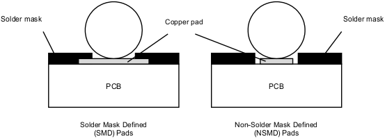
- Use Non-Solder-Mask-Defined (NSMD), rather than Solder-Mask-Defined (SMD) pads for the BGA solder balls to adhere if possible. For most applications, the NSMD pads provide more flexibility, fewer stress.
 Figure 21. Solder-Mask-Defined (SMD) and Non-Solder-Mask-Defined (NSMD) Pads
 - One trace can generally be routed between two solder pads of a 0.65 mm pitch BGA. This allows the outer two rows of solder pads to be routed on the same top/bottom layer. The TS3DDR4000 has 4 rows, and thus no VIAs is generally required to route all the inner balls out.
- Generally high-speed signal layout guidelines:
- To minimize the effects of crosstalk on adjacent traces, keep the traces at least two times the trace width apart.
- Separate high-speed signals from low-speed signals and digital from analog signals.
- Avoid right-angle bends in a trace and try to route them at least with two 45° corners.
- The high-speed differential signal traces should be routed parallel to each other as much as possible. The traces are recommended to be symmetrical.
- A solid ground plane should be placed next to the high-speed signal layer. This also provides an excellent low-inductance path for the return current flow.