SCDS216E OCTOBER 2005 – November 2017 TS5A3160
PRODUCTION DATA.
- 1 Features
- 2 Applications
- 3 Description
- 4 Revision History
- 5 Pin Configuration and Functions
-
6 Specifications
- 6.1 Absolute Maximum Ratings
- 6.2 ESD Ratings
- 6.3 Recommended Operating Conditions
- 6.4 Thermal Information
- 6.5 Electrical Characteristics for 5-V Supply
- 6.6 Electrical Characteristics for 3.3-V Supply
- 6.7 Electrical Characteristics for 2.5-V Supply
- 6.8 Electrical Characteristics for 1.8-V Supply
- 6.9 Typical Characteristics
- 7 Parameter Measurement Information
- 8 Detailed Description
- 9 Application and Implementation
- 10Power Supply Recommendations
- 11Layout
- 12Device and Documentation Support
- 13Mechanical, Packaging, and Orderable Information
11 Layout
11.1 Layout Guidelines
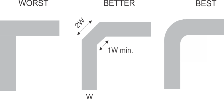
Reflections and matching are closely related to loop antenna theory, but different enough to warrant their own discussion. When a PCB trace turns a corner at a 90° angle, a reflection can occur. This is primarily due to the change of width of the trace. At the apex of the turn, the trace width is increased to 1.414 times its width. This upsets the transmission line characteristics, especially the distributed capacitance and self–inductance of the trace — resulting in the reflection. It is a given that not all PCB traces can be straight, and so they will have to turn corners. Below figure shows progressively better techniques of rounding corners. Only the last example maintains constant trace width and minimizes reflections.
Unused switch I/Os, such as NO, NC, and COM, can be left floating or tied to GND. However, the IN pin must be driven high or low. Due to partial transistor turnon when control inputs are at threshold levels, floating control inputs can cause increased ICC or unknown switch selection states.
11.2 Layout Example
 Figure 26. Trace Example