ZHCSH68G November 2017 – November 2024 UCC21220 , UCC21220A
PRODUCTION DATA
- 1
- 1 特性
- 2 应用
- 3 说明
- 4 Device Comparison Table
- 5 Pin Configuration and Functions
- 6 Specifications
- 7 Parameter Measurement Information
- 8 Detailed Description
-
9 Application and Implementation
- 9.1 Application Information
- 9.2
Typical Application
- 9.2.1 Design Requirements
- 9.2.2
Detailed Design Procedure
- 9.2.2.1 Designing INA/INB Input Filter
- 9.2.2.2 Select External Bootstrap Diode and its Series Resistor
- 9.2.2.3 Gate Driver Output Resistor
- 9.2.2.4 Estimating Gate Driver Power Loss
- 9.2.2.5 Estimating Junction Temperature
- 9.2.2.6 Selecting VCCI, VDDA/B Capacitor
- 9.2.2.7 Application Circuits with Output Stage Negative Bias
- 9.2.3 Application Curves
- 10Power Supply Recommendations
- 11Layout
- 12Device and Documentation Support
- 13Revision History
- 14Mechanical, Packaging, and Orderable Information
9.2.3 Application Curves
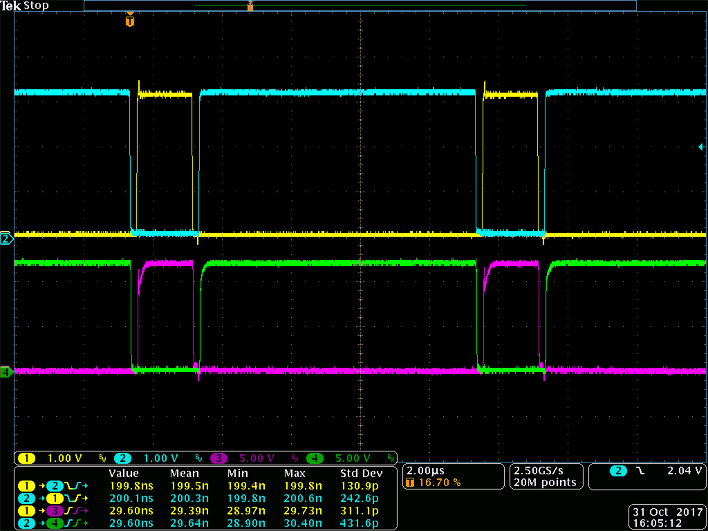
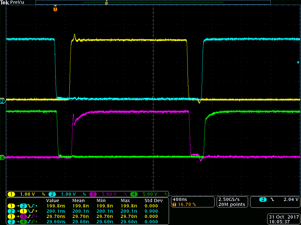
Figure 7-3 and Figure 9-6 shows the bench test waveforms for the design example shown in Figure 9-1 under these conditions: VCC = 5.0 V, VDD = 12 V, fSW = 100 kHz, VDC-Link = 400 V.
Channel 1 (Yellow): INA pin signal.
Channel 2 (Blue): INB pin signal.
Channel 3 (Pink): Gate-source signal on the high side power transistor.
Channel 4 (Green): Gate-source signal on the low side power transistor.
In Figure 9-5, INA and INB are sent complimentary 3.3-V, 20%/80% duty-cycle signals with 200ns deadtime. The gate drive signals on the power transistor have a 200-ns dead time with 400V high voltage on the DC-Link, shown in the measurement section of Figure 9-5. Note that with high voltage present, lower bandwidth differential probes are required, which limits the achievable accuracy of the measurement.
Figure 9-6 shows a zoomed-in version of the waveform of Figure 9-5, with measurements for propagation delay and deadtime. Importantly, the output waveform is measured between the power transistors’ gate and source pins, and is not measured directly from the driver's OUTA and OUTB pins.

