ZHCSF55E June 2016 – December 2021 UCC21520
PRODUCTION DATA
- 1 特性
- 2 应用
- 3 说明
- 4 Revision History
- 5 说明(续)
- 6 Pin Configuration and Functions
-
7 Specifications
- 7.1 Absolute Maximum Ratings
- 7.2 ESD Ratings
- 7.3 Recommended Operating Conditions
- 7.4 Thermal Information
- 7.5 Power Ratings
- 7.6 Insulation Specifications
- 7.7 Safety-Related Certifications
- 7.8 Safety-Limiting Values
- 7.9 Electrical Characteristics
- 7.10 Switching Characteristics
- 7.11 Insulation Characteristics Curves
- 7.12 Typical Characteristics
- 8 Parameter Measurement Information
- 9 Detailed Description
-
10Application and Implementation
- 10.1 Application Information
- 10.2
Typical Application
- 10.2.1 Design Requirements
- 10.2.2
Detailed Design Procedure
- 10.2.2.1 Designing INA/INB Input Filter
- 10.2.2.2 Select External Bootstrap Diode and its Series Resistor
- 10.2.2.3 Gate Driver Output Resistor
- 10.2.2.4 Gate to Source Resistor Selection
- 10.2.2.5 Estimate Gate Driver Power Loss
- 10.2.2.6 Estimating Junction Temperature
- 10.2.2.7 Selecting VCCI, VDDA/B Capacitor
- 10.2.2.8 Dead Time Setting Guidelines
- 10.2.2.9 Application Circuits with Output Stage Negative Bias
- 10.2.3 Application Curves
- 11Power Supply Recommendations
- 12Layout
- 13Device and Documentation Support
- 14Mechanical, Packaging, and Orderable Information
8.5 Power-up UVLO Delay to OUTPUT
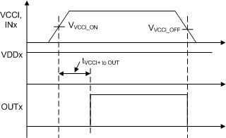
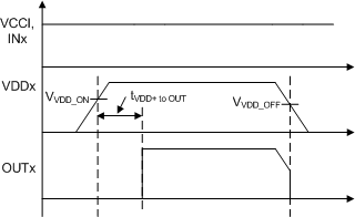
Before the driver is ready to deliver a proper output state, there is a power-up delay from the UVLO rising edge to output and it is defined as tVCCI+ to OUT for VCCI UVLO (typically 40us) and tVDD+ to OUT for VDD UVLO (typically 50us). It is recommended to consider proper margin before launching PWM signal after the driver's VCCI and VDD bias supply is ready. Figure 8-5 and Figure 8-6 show the power-up UVLO delay timing diagram for VCCI and VDD.
If INA or INB are active before VCCI or VDD have crossed above their respective on thresholds, the output will not update until tVCCI+ to OUT or tVDD+ to OUT after VCCI or VDD crossing its UVLO rising threshold. However, when either VCCI or VDD receive a voltage less than their respective off thresholds, there is <1µs delay, depending on the voltage slew rate on the supply pins, before the outputs are held low. This asymmetric delay is designed to ensure safe operation during VCCI or VDD brownouts.
 Figure 8-5 VCCI Power-up UVLO Delay
 Figure 8-6 VDDA/B Power-up UVLO Delay