ZHCSES5A March 2016 – March 2016 UCC24636
PRODUCTION DATA.
- 1 特性
- 2 应用
- 3 说明
- 4 修订历史记录
- 5 Device Comparison Table
- 6 Pin Configuration and Functions
- 7 Specifications
- 8 Detailed Description
- 9 Application and Implementation
- 10Power Supply Recommendations
- 11Layout
- 12器件和文档支持
- 13机械、封装和可订购信息
8 Detailed Description
8.1 Overview
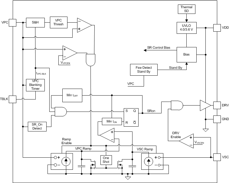
The UCC24636 SR controller is targeted for flyback converters operating in DCM and TM modes of operation. The control method to determine SR on time is based on the volt-second balance principle of primary and secondary conduction volt-second product. In converters operating in DCM and TM, the secondary current always returns to zero in each cycle. The inductor charge voltage and time product is equal to the discharge voltage and time product. The device uses internal current ramp emulators to predict the proper SR on time based on voltage and time information on the VPC and VSC pins.
To achieve very low standby power in the converter, the UCC24636 has a standby mode of operation that disables the SR MOSFET drive and reduces the device bias current to ISTBY. The device monitors the average switching frequency of the converter to enter and exit the standby mode of operation, and is compatible with converters operating in burst mode or constant frequency in light-load mode.
8.2 Functional Block Diagram
8.3 Feature Description
8.3.1 Start Up and UVLO
The UCC24636 features a wide operating VDD range and low UVLO thresholds. The start up of the device is dependent on voltage levels on three pins: VDD, VPC and VSC. The VDD pin can be directly connected to the power supply output on converters from 5-V to 24-V nominal outputs. The start UVLO threshold is VVDD(on), 4.0 V typical, and stop threshold is VVDD(off), 3.6 V typical. The DRV output is not enabled unless the voltage on the VPC pin is greater than VVPCEN for a time longer than tVPC-BLK and the voltage on the VSC pin is greater than VVSCEN. Once the VDD, VSC and VPC voltage and time thresholds are met, there is an internal initialization time before the DRV output is enabled.
Refer to Figure 12 for a startup sequence that illustrates the timing sequence and configurable DRV output based on VDD level. In most converter designs, the conditions for the VPC and VSC voltage to enable the device are met before the VDD start-voltage threshold, this is reflected in the timing diagram. When VDD exceeds VVDD(on) UVLO threshold the device starts the initialization sequence of 150 µs to 250 µs illustrated as tINITIALIZE. After the device initialization, there is a logic initialization of 20 µs at which time VTBLK is enabled (high). At VDD < VPMOS the driver high-side PMOS device is enabled and the DRV peak will be close to VDD. When VDD exceeds VPMOS the PMOS device is disabled and the driver is operating as a high-side NMOS only and DRV is approximately 1.2 V to 1.5 V lower than VDD. As VDD continues to increase, the DRV output is limited to VDRCL regardless of VDD up to the recommended maximum rating.
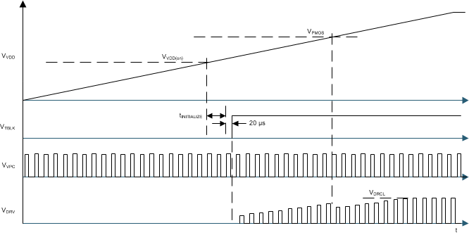 Figure 12. Start-Up Operation
8.3.2 Volt-Sec SR Driver On-Time Control
Refer to the timing diagrams in Figure 13 for functional details of the UCC24636 volt-sec on-time control.
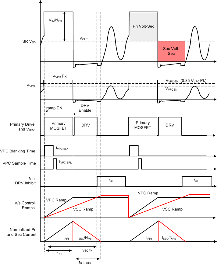 Figure 13. Operation in DCM
The UCC24636 uses the VPC and VSC pins to sense the SR MOSFET VDS voltage and converter VOUT voltage through resistor dividers. The information of VIN/NPS, tPRI, and VOUT can be obtained from the information on VPC and VSC pins. The SR MOSFET turn on is determined when the SR MOSFET body diode starts conducting and the VPC pin voltage falls to near zero; the SR MOSFET turn off is determined by the current emulator control ramps.
The UCC24636 volt-sec control generates the internal VPC ramp and VSC ramp to emulate the transformer Volt-Sec balancing as shown in Figure 13.
The secondary current discharge time, tSEC-DIS can be determined indirectly. The primary volt-sec ramp and secondary volt-sec ramp both start when VPC rises above VVPC-EN and VVPC-TH. The charge currents for the VPC and VSC ramps are determined by the voltage on the VPC and VSC pins respectively.
When VPC is higher than VVPC-EN and VVPC-TH for t > tVPC-BLK, the VPC pulse is qualified as a primary conduction pulse and the SR can be enabled on the VPC falling edge. The VPC ramp continues to rise until the VPC falling edge based on the real time voltage on the VPC pin and holds the peak for the cycle. The DRV output is turned on during the VPC falling edge near zero volts, and DRV is turned off when the VSC rising ramp crosses the VPC ramp held level.
Both VPC and VSC ramps are reset to zero on each VPC rising edge above the VVPC-EN and VVPC-TH thresholds.
To discriminate primary on-time pulses from DCM ringing, there are voltage and time criteria that must be satisfied on the VPC pin to enable the DRV output. tVPC-BLK can be adjusted through the resistor on TBLK pin.
At the rising edge of VPC when the voltage exceeds VVPC-EN and VVPC-TH the blanking time tVPC-BLK is initiated. At the end of tVPC-BLK, the VPC voltage is sampled during tVPC-SPL window, which is 100 ns nominal. Also at the end of tVPC-BLK, the DRV output can be enabled.
The VPC voltage sampled during tVPC-SPL determines the VPC dynamic threshold VVPC-TH which is normally 85% of the sampled VPC voltage. The dynamic threshold provides the ability to reject the DCM ringing and detect the primary on-time. Noise immunity during the turn-on event of DRV at the falling edge of the VPC pin is enhanced by a minimum DRV on time of tSRONMIN, which is 350 ns nominal.
During the falling edge of DRV, the tOFF timer is initiated which inhibits turn on of the SR until tOFF expires. This eliminates false turn on of DRV if the DCM ringing is close to ground.
The UCC24636 is designed to operate in a variety of flyback converter applications over a wide operating range. The internal volt-sec control ramps do have a dynamic range limit based on volt-sec on the VPC pin. As shown in Figure 14, a Volt-sec product exceeding 7 V-µs on the VPC pin will result in saturation of the VPC volt-sec control ramp. Operation beyond this point results in a DRV on-time less than expected. For example, if VVPC = 0.5 V, tVPC should be < 14 µs, or if VVPC = 2.0 V, tVPC should be < 3.5 µs, to operate within the dynamic range of the device. Assuming a converter operating in transition mode at low line and full load with a 50% duty cycle, the operating period is 28 µs which results in a frequency that is under 40 kHz. The UCC24636 low-frequency operating range extends to the standby mode threshold of 5 kHz; but each switching cycle VVPC Volt-sec product should be less than 7 V-µs.
The device can support switching frequencies exceeding 130 kHz but the following timing limits need to be confirmed to be compatible with the power train. The minimum primary on time when the device is expected to be active needs to be compatible with the minimum VPC blanking time (tVPC-BLK) setting of 203 ns plus the sampling window (tVPC-SPL) of 100 ns. The minimum secondary current conduction time should be greater than the minimum SR on time (tSRONMIN) of 350 ns. The minimum time from the SR drive turn off until the next SR drive turn on should be greater than the SR minimum off time (tOFF) of 4.35 µs.
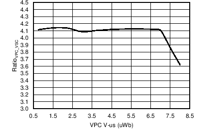 Figure 14. RatioVPC_VSC vs VPC V-µs
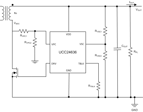 Figure 15. SR Controller Components
Determining the VPC and VSC divider resistors is based on the operating voltage ranges of the converter and RatioVPC-VSC gain ratio. Referring to Figure 15, the following equation determines the VPC divider values.
For RVPC2, a value of 10 kΩ is recommended for minimal impact on time delay, and low-resistor dissipation. A higher RVPC2 value reduces resistor divider dissipation but may increase the DRV turn-on delay due to the time constant of ~2 pF pin capacitance and divider resistance. A lower RVPC2 value can be used with the tradeoff of higher dissipation in the resistor divider. A factor of 10% over the VPC threshold, VVPCEN, is shown in Equation 1 for design margin.

where
- VIN(min) is the converter minimum primary bulk capacitor voltage.
- VOUT(min) is the minimum converter output voltage in normal operation.
- VVPCEN is the VPC enable threshold, use the specified maximum value.
- NPS is the transformer primary to secondary turns ratio.
The operating voltage range on the VPC pin should be within the range of 0.45 V < VVPC < 2.2 V. Referring to Figure 6, if VVPC is greater than 2.3 V the linear dynamic range is exceeded and RatioVPC_VSC is reduced; in this condition the DRV on time is less than expected. If VVPC is greater than 2.6 V for 500 ns, a fault is generated and DRV is disabled for the cycle, refer to Pin Fault Protection. To ensure the maximum voltage is within range confirm with Equation 2.

where
- VIN(max) is the converter maximum primary bulk capacitor voltage.
- VOUT(max) is the maximum converter output voltage at OVP.
- NPS is the transformer primary-to-secondary turns ratio.
The program voltage on the VSC pin is determined by the VPC divider ratio and the device's parameter RatioVPC_VSC. The current emulator ramp gain is higher on the VPC pin by the multiple RatioVPC_VSC, so the VSC resistor divider ratio is reduced by the same RatioVPC_VSC accordingly. Determine the VSC divider resistors using Equation 3 below. To minimize resistor divider dissipation, a recommended range for RVSC2 is 25 kΩ to 50 kΩ. Higher RVSC2 values results in increasing offset due to VSC input current, IVSC. Lower RVSC2 values increases the resistor divider dissipation. To ensure DRV turn off slightly before the secondary current reaches zero, 10% margin is shown for initial values. Use a nominal value of 4.15 for RatioVPC_VSC.

where
- RatioVPC_VSC is the device parameter VPC and VSC gain ratio, use a value of 4.15.
The operating voltage on the VSC pin should be within the range of 0.3 V < VVSC < 2.2 V. Referring to Figure 7, if VVSC is greater than 2.3 V, the linear dynamic range is exceeded and RatioVPC_VSC is increased; in this condition the DRV on time is more than expected, resulting in possible negative current conduction. To ensure the VSC voltage is within range, confirm with Equation 4 and Equation 5.


where
- VOUT(min) is the minimum converter output operating voltage of the SR controller.
- VOUT(max) is the maximum converter output operating voltage of the voltage at OVP.
Discrimination of ringing during DCM operation from valid primary on-time is achieved by a dynamic VPC rising threshold and programmable blanking time. The dynamic threshold VVPC-TH is 85% typical ratio of the previous VPC pin peak voltage. Referring to Figure 13, the VPC pin voltage is sampled after the VPC voltage is greater than VVPCEN and VVPC-TH for t > tVPC-BLK. The function of the dynamic threshold VVPC-TH is to reject the ringing in DCM operation from the primary conduction pulses. The dynamic threshold has an active range from the minimum VVPCEN voltage to a maximum of 1-V clamp. The blanking time is programmable from 200 ns to 2 µs in order to accommodate a variety of converter designs.
Refer to Figure 16 for guidance on selecting the blanking time. The blanking time should be selected as long as reasonable and still accommodate the minimum primary on-time at light-load condition and high-line voltage. In the high-line minimum load condition, select a blanking time that meets the following criteria (Equation 6) to accommodate tolerance of the blanking time and the tVPC-SPL sampling time window.
For rejection of DCM ringing, the blanking time should be longer than the time that the ring is above the VVPC-TH dynamic threshold, which is 85% of the minimum SR VDS peak voltage. Determine these criteria at low line and maximum load condition. It is recommended that the transformer turns ratio be selected such that the secondary reflected voltage is < 85% of VIN(min) bulk capacitor voltage at the highest load when DCM operation occurs at the low line input condition.
To determine the resistor value for tVPC-BLK use Equation 7 to select from a range of 200 ns to 2 µs.

where
- tVPC-BLK is the target blanking time.
Additional discrimination for proper SR timing control is provided by the tOFF function. Refer to Figure 13 for the timing details. After the DRV turn off, the DRV is inhibited from turning on again until the tOFF timer expires. This protects against SR false turn on from SR VDS DCM ringing below ground.
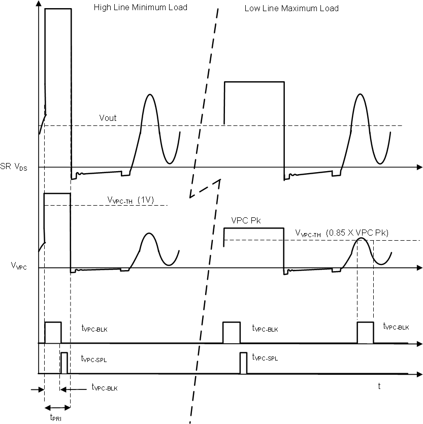 Figure 16. VPC Blanking Time Criteria
8.3.3 Standby Operation
To minimize power consumption at very light load and standby conditions, the UCC24636 disables the SR DRV output and enters a low current operating state. The criteria for operating in standby mode or normal operation are determined by the average frequency detected on the VPC pin. The frequency detection is compatible with burst mode operation or continuous low frequency FM operation. At start up the device is in normal operation to enable DRV to the SR MOSFET. If < 64 cycles occur in tENTO,12.8 ms typical, the device disables the DRV output and enters low-current operating mode with bias current of ISTBY. In standby mode the criteria to enter normal operating mode is when > 32 cycles occur within tEN, 2.56 ms typical. The device enters normal operation as soon as the 32 cycles occur to reduce the response time exiting standby operation. The average frequency of entering standby mode is 5 kHz typical, and the average frequency of exiting standby mode is 12.5 kHz typical. Refer to Figure 17 for an illustration of standby mode timing.
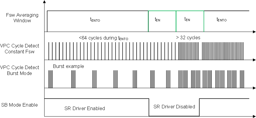 Figure 17. Standby Mode Operation
8.3.4 Pin Fault Protection
The UCC24636 controller includes fault protection in the event of open pin, shorted pin to ground and abnormal out of range operation.
8.3.4.1 VPC Pin Overvoltage
In the event that there is an abnormal high level on the VPC pin for a period beyond expected transformer leakage spike duration, the DRV output is disabled on a cycle-to-cycle basis. If the voltage on the VPC pin exceeds VVPCDIS, 2.6 V minimum, for 500 ns the SR is not enabled until the next valid cycle.
8.3.4.2 VPC Pin Open
In the event of an open circuit VPC pin, the device defaults to a zero VPC input signal condition which results in disabling DRV operation.
8.3.4.3 VSC Pin Open
In the event of an open circuit VSC pin, the device defaults to a zero VSC input signal condition which results in disabling DRV operation.
8.3.4.4 TBLK Pin Open
In the event of an open circuit TBLK pin, the device disables DRV operation.
8.3.4.5 VPC and VSC Short to Ground
Since the VPC and VSC enable thresholds must be satisfied for DRV operation, DRV is inherently disabled.
8.3.4.6 TBLK Pin Short to Ground
A shorted TBLK pin results in a minimum setting for tVPC-BLK blanking time.
8.4 Device Functional Modes
According to VDD voltage, VSC voltage, and VPC voltage and frequency, the device can operate in different modes.
8.4.1 Start-Up
During start-up when VDD is less than VVDD(on) the device is disabled. When VDD exceeds the VVDD(on) UVLO threshold the IDD goes to IRUN and the device begins the start sequence detailed in Start Up and UVLO.
8.4.2 Normal Operation
When VDD exceeds VVDD(on), the VPC voltage exceeds VVPC-EN and VVPC-TH, and the VSC voltage exceeds VVSCEN the DRV output is active. If the switching frequency is above the standby criteria of > 5 kHz the device is in normal operation determining the DRV time based on volt-sec control. IDD will be IRUN.
- The device operates in volt-sec control based on the VPC and VSC volt-sec control ramps.
8.4.3 Standby Operation
If the number of VPC pulses is less than nENTO, 64, during tENTO the device enters standby mode. DRV operation stops and most device functions are shut down. IDD is ISTBY during standby operation. To exit standby mode the number of VPC pulses must exceed nEN, 32, during tEN. IDD returns to IRUN and the DRV output starts after the initialization time as outlined in Figure 12.
8.4.4 Conditions to Stop Operation
The following conditions can disable DRV operation; IDD is IRUN during these conditions.
- VPC overvoltage: When VVPC > VVPCDIS for >500 ns the DRV output is disabled for the cycle.
- VSC undervoltage: When VVSC < VVSCEN, the DRV output is disabled.
- VPC undervoltage: When VVPC< VVPCEN, the DRV output is disabled.