ZHCSJY8E june 2019 – february 2021 UCC256402 , UCC256403 , UCC256404
PRODUCTION DATA
- 1 特性
- 2 应用
- 3 说明
- 4 Revision History
- 5 Pin Configuration and Functions
- 6 Specifications
-
7 Detailed Description
- 7.1 Overview
- 7.2 Functional Block Diagram
- 7.3 Feature Description
- 7.4
Device Functional Modes
- 7.4.1 High Voltage Start-Up
- 7.4.2 X-Capacitor Discharge
- 7.4.3 Burst Mode Control
- 7.4.4
System State Machine
-
Application and Implementation
- 8.1 Application Information
- 8.2
Typical Application
- 8.2.1 Design Requirements
- 8.2.2
Detailed Design Procedure
- 8.2.2.1 LLC Power Stage Requirements
- 8.2.2.2 LLC Gain Range
- 8.2.2.3 Select Ln and Qe
- 8.2.2.4 Determine Equivalent Load Resistance
- 8.2.2.5 Determine Component Parameters for LLC Resonant Circuit
- 8.2.2.6 LLC Primary-Side Currents
- 8.2.2.7 LLC Secondary-Side Currents
- 8.2.2.8 LLC Transformer
- 8.2.2.9 LLC Resonant Inductor
- 8.2.2.10 LLC Resonant Capacitor
- 8.2.2.11 LLC Primary-Side MOSFETs
- 8.2.2.12 LLC Rectifier Diodes
- 8.2.2.13 LLC Output Capacitors
- 8.2.2.14 HV Pin Series Resistors
- 8.2.2.15 BLK Pin Voltage Divider
- 8.2.2.16 ISNS Pin Differentiator
- 8.2.2.17 VCR Pin Capacitor Divider
- 8.2.2.18 BW Pin Voltage Divider
- 8.2.2.19 Soft Start and Burst Mode Programming
- 8.2.3 Application Curves
-
Application and Implementation
- 8 Power Supply Recommendations
- 9 Layout
- 10Device and Documentation Support
7.3.7 Output Voltage Sensing
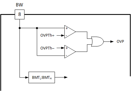
The output voltage is sensed through the bias winding (BW) voltage sense pin. With one terminal of the bias winding connected to primary side ground, the bias winding voltage at the other terminal represents the output voltage when the secondary side rectifier diode conducts. A resistor divider is typically used to connect from the bias winding terminal to the BW pin. The BW voltage is compared with a positive and a negtive threshold to generate an output OVP fault. During startup, BW pin is multiplexed for burst mode threshold programming. The details are introduced in the Section 7.4.3.1 section. The block diagram of the bias winding voltage sense block is shown below.
 Figure 7-9 Bias Winding Sensing Block Diagram
If the OVP event is high for 5 consecutive switching cycles, the system will enter FAULT state. The actions during an OVP fault are described in the Section 7.3.9.3 section.