ZHCSTY3I September 2008 – November 2023 UCC27423-Q1 , UCC27424-Q1 , UCC27425-Q1
PRODUCTION DATA
- 1
- 1 特性
- 2 应用
- 3 说明
- 4 Device Comparison Table
- 5 Pin Configuration and Functions
- 6 Specifications
- 7 Detailed Description
- 8 Application and Implementation
- 9 Power Supply Recommendations
- 10Layout
- 11Device and Documentation Support
- 12Revision History
- 13Mechanical, Packaging, and Orderable Information
封装选项
机械数据 (封装 | 引脚)
散热焊盘机械数据 (封装 | 引脚)
- DGN|8
订购信息
7.3.5 Operational Waveforms and Circuit Layout
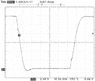
Figure 7-2 shows the circuit performance achievable with a single driver (half of the 8-pin IC) driving a 10-nF load. The input pulse width (not shown) is set to 300 ns to show both transitions in the output waveform. Note the linear rise and fall edges of the switching waveforms. This is due to the constant output current characteristic of the driver as opposed to the resistive output impedance of traditional MOSFET-based gate drivers.
 Figure 7-2 Pulse Response
In a power driver operating at high frequency, it is a significant challenge to get clean waveforms without much overshoot or undershoot and ringing. The low output impedance of these drivers produces waveforms with high di/dt. This tends to induce ringing in the parasitic inductances. Use the upmost care in the circuit layout. It is advantageous to connect the driver IC as close as possible to the leads. The driver IC layout has ground on the opposite side of the output, so the ground must be connected to the bypass capacitors and the load with copper trace as wide as possible. These connections must also be made with a small enclosed loop area to minimize the inductance.