ZHCSTY3I September 2008 – November 2023 UCC27423-Q1 , UCC27424-Q1 , UCC27425-Q1
PRODUCTION DATA
- 1
- 1 特性
- 2 应用
- 3 说明
- 4 Device Comparison Table
- 5 Pin Configuration and Functions
- 6 Specifications
- 7 Detailed Description
- 8 Application and Implementation
- 9 Power Supply Recommendations
- 10Layout
- 11Device and Documentation Support
- 12Revision History
- 13Mechanical, Packaging, and Orderable Information
封装选项
机械数据 (封装 | 引脚)
散热焊盘机械数据 (封装 | 引脚)
- DGN|8
订购信息
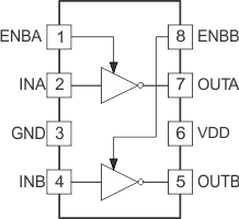
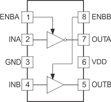
5 Pin Configuration and Functions
 Figure 5-1 UCC27423-Q1: D or DGN Package8-Pin SOIC
or MSOP With PowerPADDual Inverting, Top
View
 Figure 5-2 UCC27424-Q1: D or DGN Package8-Pin SOIC
or MSOP With PowerPADDual Noninverting,
Top View
 Figure 5-3 UCC27425-Q1: D Package8-Pin
SOICOne Inverting, One Noninverting, Top
View
Figure 5-3 UCC27425-Q1: D Package8-Pin
SOICOne Inverting, One Noninverting, Top
ViewTable 5-1 Pin Functions
| PIN | I/O | DESCRIPTION | |
|---|---|---|---|
| NO. | NAME | ||
| 1 | ENBA | I | Enable input for the driver A with logic-compatible threshold and hysteresis. The driver output can be enabled and disabled with this pin. It is internally pulled up to VDD with 100-kΩ resistor for active high operation. The output state when the device is disabled is low, regardless of the input state. |
| 2 | INA | I | Input A. Input signal of the A driver which has logic-compatible threshold and hysteresis. If not used, this input must be tied to either VDD or GND. It must not be left floating. |
| 3 | GND | — | Common ground. This ground must be connected very closely to the source of the power MOSFET which the driver is driving. |
| 4 | INB | I | Input B. Input signal of the B driver which has logic-compatible threshold and hysteresis. If not used, this input must be tied to either VDD or GND. It must not be left floating. |
| 5 | OUTB | O | Driver output B. The output stage is capable of providing 4-A drive current to the gate of a power MOSFET. |
| 6 | VDD | — | Supply voltage and the power input connection for this device. |
| 7 | OUTA | O | Driver output A. The output stage is capable of providing 4-A drive current to the gate of a power MOSFET. |
| 8 | ENBB | I | Enable input for the driver B with logic-compatible threshold and hysteresis. The driver output can be enabled and disabled with this pin. It is internally pulled up to VDD with 100-kΩ resistor for active-high operation. The output state when the device is disabled is low, regardless of the input state. |